

AN-2619: 多摩川アブソリュート・エンコーダ・プロトコルのTMC8100 向けサポート
説明
TMC8100 は、最大16Mbit/s のシリアル同期/非同期アブソリュート・エンコーダ・プロトコル用に最適化された、プログラマブル・マイクロコントローラを内蔵しています。このデバイスは、専用のエンコーダ・プロトコル・インターフェースIC やFPGA 実装に代えて使用できる一方で、様々なエンコーダ機能のシステム内アップデートや、他のエンコーダ・プロトコルへの切り替えもサポートしています。TMC8100 は小型でコスト効率に優れ、なおかつ柔軟な通信ソリューションであり、工業用ドライブにアブソリュート・エンコーダのサポート機能を追加します。
このアプリケーション・ノートでは、多摩川精機製アブソリュート・エンコーダをサポートするTMC8100 ソフトウェアのリファレンス実装に関する詳細を示します。
特長
- 多摩川精機のT-Format を実装
- 2.5Mbps のアブソリュート・エンコーダをサポート
- データ読出しとオンザフライ冗長巡回検査/CRCチェックサム計算をサポート
アプリケーション
- サーボ・ドライブの位置フィードバック
- サーボ・ドライブのモータ制御

システムの説明
工業用アプリケーションなどに用いられるサーボ・モータ・ドライブには、正確で信頼性が高く、しかも低レイテンシの位置フィードバックが必要です。これまで長期にわたり、インクリメンタルA/B/N 出力の光エンコーダが業界標準として使われてきました。その一方でアブソリュート・ポジション・エンコーダも多用されるようになっていますが、その多くは機能を追加し、異なるインターフェース・プロトコル(ほとんどがベンダー固有)を使っています。その一例が多摩川精機のT-Format プロトコルで、これはエンコーダとコントローラ間でのデジタル・データのシリアル転送に使われます。物理層はRS485 規格に基づいています。位置の値と診断情報を送信することができる他、エンコーダが内蔵するメモリの読出しと書込みが可能です。
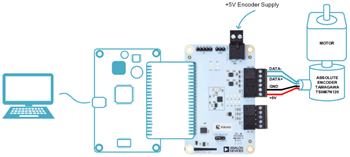
T-Format プロトコル使用のエンコーダは、シングルシールドの4 線式ケーブルを介してTMC8100-EVAL-KIT に接続します(図1)。4 線の内訳は次のとおりです。
- +5V とGND:エンコーダの電源とグラウンド接続
- DATA+とDATA−:データ通信(双方向)用の差動RS485 信号
リファレンス実装は次のような機能を備えています。
- T-Format プロトコルと同じ2.5Mbps のデータ・レートをサポート
- コマンド(ID0、ID1、ID2、ID3、ID6、ID7、ID8、IDC、IDD)を送信して応答を受信
- データのパッキングとパッキング解除
- CRC チェックサムのオンザフライ計算、送信データへの付加
- CRC チェックサムのオンザフライ計算、受信CRC との比較
リファレンス実装はソース・コードで提供されます。ユーザはこれを出発点として使用し、アプリケーションの必要に応じて変更を加えることができます。
システムの概要
提供されるソフトウェアはTMC8100-EVAL-KIT と共に使用するように設計されており、多摩川精機のTS5667N120 エンコーダを使ってテストされています。

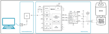
TMC8100-EVAL-KIT に使われているコア・ハードウェア・コンポーネントは、TMC8100 とRS485 トランシーバです。RS485 トランシーバは、DATA+およびDATA−信号としてコネクタに送られてくる差動RS485 信号とTMC8100 の信号間の変換に使用します(図2)。
ソフトウェアには、このプロトコルをサポートするためのコントローラ機能を実装したTMC8100 のファームウェアが含まれています。このファームウェアは、パワーアップ後にTMC8100 にダウンロードする必要があります。ファームウェアの選択とダウンロード、およびその後のファームウェア機能のデモとテストのための追加GUI は、Python スクリプトとして提供されています。
多摩川精機のT-Format プロトコル
多摩川精機はエンコーダ技術を基盤とするメーカーです。エンコーダには、位置出力がインクリメンタル方式のものとアブソリュート方式のものがあります。このリファレンス実装は、RS485 ライン・ドライバを使い、デジタル出力で絶対位置情報を提供するエンコーダに焦点を合わせています。通信に使われるこのプロトコル・フォーマットはT-Format と呼ばれます。
T-Format を使用するエンコーダとの通信は、通常、コントローラからエンコーダに送られる要求と、次の要求を送信する前にエンコーダからコントローラに送り返される応答で構成されます。
この通信プロトコルは大まかに3 種類の要求に分類できます。データ読出し、リセット、および組込みEEPROM(電気的に消去可能なプログラマブル読出し専用メモリ)へのアクセスです。これらの異なる要求は、固有のID コードによって識別されます。
| TRANSACTION TYPE | ID CODE | DESCRIPTION |
| Data Readout | 0 | Absolute data in one revolution (ABS) |
| 1 | Multiturn data (ABM) | |
| 2 | Encoder ID (ENID) | |
| 3 | ABS + ABM + ENID + Encoder error status (ALMC) | |
| EEPROM Write | 6 | Write EEPROM [Address (ADF) and Data (EDF)] |
| EEPROM Read | D | Read EEPROM [Address (ADF)] |
| Reset | 7 | Reset ABS value |
| 8 | Reset ABM value | |
| C | Reset Errors |
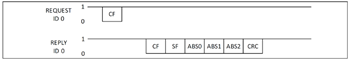
データ読出しの場合、TMC8100 はコントロール・フィールド(CF)データグラムをエンコーダに送信し(表2)、エンコーダは、このCFのコピー、ステータス・フィールド(SF)、要求に応じたいくつかのデータ・フィールド、およびCRC チェックサム(CRC)(表3)で応答します。EEPROM への書込みの場合、TMC8100 はCF を送信し、その後にEEPROM アドレス・フィールド(ADF)、EEPROM データ・フィールド(EDF)、およびCRC を続けます。EEPROM の読出しは、コントロール・フィールド(CF)、EEPROM アドレス・フィールド(ADF)、およびCRC で構成されます。どちらの場合も、エンコーダはEEPROM ADF、EEPROM データ・フィールド/EDF、およびCRC チェックサムで応答します。リセットの場合、TMC8100 はCF を送信し、応答には常に1 回転以内のエンコーダの絶対位置(ABS)が含まれます。
| ID CODE | TRANSACTION TYPE | FIELDS TRANSMITTED TMC8100 | |||
| 0 | Data Readout | CF | |||
| 1 | Data Readout | CF | |||
| 2 | Data Readout | CF | |||
| 3 | Data Readout | CF | |||
| 6 | EEPROM Write | CF | ADF | EDF | CRC |
| D | EEPROM Read | CF | ADF | CRC | |
| 7 | Reset | CF | |||
| 8 | Reset | CF | |||
| C | Reset | CF | |||
CF:コントロール・フィールド
ADF:EEPROMアドレス・フィールド
EDF:EEPROM データ・フィールド
CRC:CRC フィールド
| ID CODE | TRANSACTION TYPE | FIELDS TRANSMITTED (ENCODER) | ||||||||||
| 0 | Data Readout | CF | SF | ABS0 | ABS1 | ABS2 | CRC | |||||
| 1 | Data Readout | CF | SF | ABM0 | ABM1 | ABM2 | CRC | |||||
| 2 | Data Readout | CF | SF | ENID | CRC | |||||||
| 3 | Data Readout | CF | SF | ABS0 | ABS1 | ABS2 | ENID | ABM0 | ABM1 | ABM2 | ALMC | CRC |
| 6 | EEPROM Write | CF | ADF | EDF | CRC | |||||||
| D | EEPORM Read | CF | ADF | EDF | CRC | |||||||
| 7 | Reset | CF | SF | ABS0 | ABS1 | ABS2 | CRC | |||||
| 8 | Reset | CF | SF | ABS0 | ABS1 | ABS2 | CRC | |||||
| C | Reset | CF | SF | ABS0 | ABS1 | ABS2 | CRC | |||||
ABS:1 回転以内の絶対位置
ABM:マルチターン位置
ENID:エンコーダID
ALMC:エンコーダ・エラー
一例として、1 回転以内(ID コード0)のエンコーダ絶対位置の読出しの要求と応答を図3 に示します。

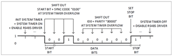
通信は非同期です。各フィールドは10 ビットで構成されます。内訳は1 スタート・ビット、LSB ファーストの8 ビット・データ、1 ストップ・ビットです。
CF には、スタート・ビット、3 つの同期ビット、ID コード(この例ではID コード0)、およびストップ・ビットが含まれています(図4)。


エンコーダの絶対位置はその後に続く3 バイトABS0~ABS2 に分割され、最下位バイトが最初に送信されます(図5)。


最後のデータ・フィールドの後に送信されるCRC コードは、スタート・ビットとストップ・ビットを除くCF 内の8 ビット、ステータス・フィールド(SF)、およびデータ・フィールド(ABS0、ABS1、ABS2)が対象で、これらのフィールドを保護します(図6)。


このセクションではT-Format プロトコルの概要を示します。詳細は多摩川精機が提供する仕様を参照してください。
ソフトウェアの概要
TMC8100 用多摩川プロトコルのファームウェア実装は、ソース・コード「tmc8100-eval_tamagawa_encoder_demo_v10.asm」と、Intel 16 進ファイル・フォーマットの機械語コード「tmc8100-eval_tamagawa_encoder_demo_v10.hex」で提供されます。機能の最初のテスト/評価用には、「tmc8100-eval_tamagawa_encoder_demo_v10.py」というPython スクリプトを使用できます。これは、図1 に示す要領でエンコーダを取り付けたTMC8100-EVAL-KIT にUSB を介して接続されたPC 上で実行できます。
Python スクリプト・プログラムを実行するには、まずPython インタープリタをPC にインストールして、「intelhex」および「pySerial」というPython ライブラリを使用する必要があります。このスクリプトは、グラフィカル・ユーザ・インターフェース用の「tkinter」を使用します。
TMC8100-EVAL-KIT にエンコーダを接続してUSB でPC に接続し、TMC8100-EVAL-KIT に+5V を加えると、以下のようにコマンド・ラインからPython スクリプトを実行できます。


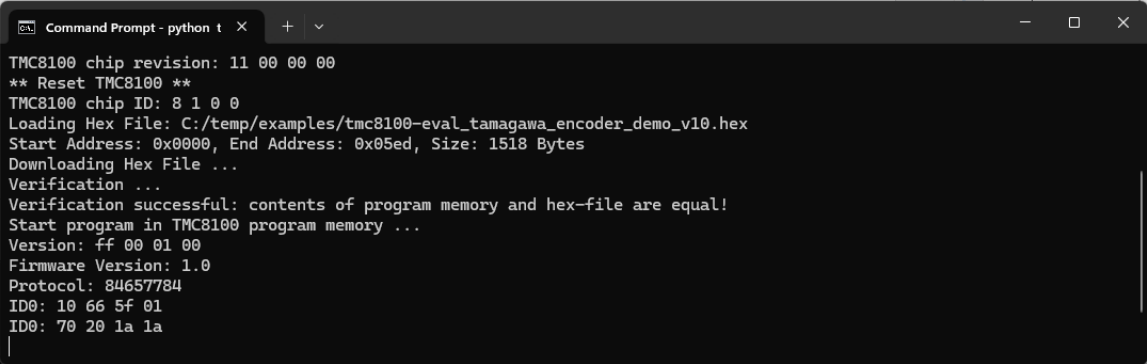
最初に、TMC8100-EVAL-KIT へのUSB 接続に使用する仮想COM ポートを選ぶ必要があります。この例では「COM4」です。ターミナル・ウィンドウに表示された出力行には、既にLandungsbruecke(LB)への接続に成功してTMC8100 を検出したこと、およびそのチップID とリビジョン番号が示されます。
その後、別のウィンドウでGUI が自動的に起動します。


まず、[Select Input File]フレームの[…]ボタン(1)を使い、TMC8100 用のサンプル・コードが格納された16 進ファイル「tmc8100-eval_tamagawa_encoder_demo_v10.hex」を選択します。その後に「Load + Execute」ボタン(2)を押すと、ブートローダによりファイルの設定内容がUSB とLandungsbruecke/LB を介してTMC8100 のSRAM プログラム・メモリに書き込まれて、プログラムが実行されます。このプログラムは、固有の通信プロトコルを使用してエンコーダにアクセスします。例えば同じプログラムや異なるプログラムをダウンロードするためにTMC8100 を再びブートローダ・モードにするには、リセットまたは電源サイクルを行う必要があります。


ウィンドウの中央にある[Tamagawa T-Format]フレームの左側には、異なるコマンド(ID0~IDD)がそれぞれ異なるボタンとして配置されています。[ID0]ボタンを押すとこれに対応するコマンドが送られて、エンコーダから1 回転内の絶対位置([ABS]ラベルの隣に表示)とステータス・フラグ([SF]ラベルの隣に表示)が返されます。エンコーダから受信したCRCチェックサムと、シリアル・データの受信時に並行してTMC8100 が計算したチェックサムは、それぞれ[CRC received]ラベルと[CRC calculated]ラベルの隣に表示されます。
抽出/関連データの表示されるGUI と並行して、コマンド・ライン・ウィンドウには未加工通信データといくつかの追加情報が表示されます。これらのデータと情報は、TMC8100 のサンプル・プログラムを変更/拡張する際に役立ちます。

ファームウェア実装
サンプル・ソース・コード「tmc8100-eval_tamagawa_encoder_demo_v10.asm」は出発点として使用できるほか、アプリケーションの要求に応じて変更を加えることができます。アセンブラ(Assembler)は、ソース・コードの変換に使用できます。
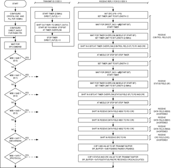
ID コード0 コマンドの送信と応答の受信に焦点を当てたサンプル・コードの概要をフローチャート(図7)に示します。
ファームウェアのソース・コードは、可読性向上のために、いくつかの値(例えばソフトウェア・バージョンとサポートされているプロトコル)の定義と、TMC8100 内にある周辺装置のレジスタ・アドレスの定義から始まります。
SOFTWARE_VERSION_MAJOR = $01
 SOFTWARE_VERSION_MINOR = $00
 PROTOCOL_3 = $54 ; "T"
 PROTOCOL_2 = $41 ; "A"
 PROTOCOL_1 = $4D ; "M"
 PROTOCOL_0 = $54 ; "T"
 . . . .
 ; spi register address
 SPI_BUFFER_0 = $30

クロックの選択と初期化
TMC8100 は常に内部発振器で起動し、パワーオン/リセット後にブートローダが75MHz のシステム・クロック周波数でPLL を設定します。多摩川プロトコルには、より高精度のクロック・ソースが必要です。この例では、TMC8100-EVAL-KIT に搭載された16MHz の水晶を使用する発振器が使われています。もちろん外部クロックを使用することもできます。PLL 出力とシステム周波数は、その後のクロック計算/分周設定を容易にするために、100MHz に設定されています。
最初のステップとして、GPIO0 とGPIO1 を内部水晶発振器との併用で外部水晶用に設定します。
LDI $03, r0 ; enable input for GPIO0/GPIO1
 ST GPIO_IN, r0

 LDI $03, r0 ; disable pull-up for GPIO0/GPIO1
 ST GPIO_PU, r0
次のステップでは、100MHz のPLL 出力周波数(PLL_FB_100)と水晶発振器(XTAL)クロック回路に合わせてPLL フィードバック分周器が設定され、PLL 入力におけるクロック周波数が1MHz となるようにPLL 入力分周器が設定されます。クロック・ブロックのアドレスはレジスタごとに間接的に指定されるので、書込みアクセスには4 つのコマンドが必要です。まずロード命令(LDI)とストア命令(ST)のペアでレジスタ・アドレスを設定し、その後にもう1 つのロード命令とストア命令のペアで新しいレジスタ値を設定します。
LDI PLL_FB_CFG, r0 ; set pll feedback divider
 ST CLK_ADDR, r0
 LDI PLL_FB_100, r0
 ST CLK_DOUT, r0 ; will trigger write access to clk register

 LDI CLK_CTRL_SOURCE, r0
 ST CLK_ADDR, r0
 LDI $26, r0 ; use XTAL
 ST CLK_DOUT, r0 ; will trigger write access to clk register

 LDI CLK_CTRL_OPT, r0 ; enable clk fsm
 ST CLK_ADDR, r0
 LDI $40, r0
 ST CLK_DOUT, r0 ; will trigger write access to clk register

 LDI CLK_CTRL_PLL_CFG, r0
 ST CLK_ADDR, r0
 LDI %1011_1101, r0 ; RDIV = 15 (assuming 16MHz external / XTAL clock)
 ; and select PLL output, start FSM (commit = 1)
 ST CLK_DOUT, r0 ; will trigger write access to clk register
最後の書込みアクセスは、すべての変更を適用するためにクロック・ブロックの内部ステート・マシンもトリガします。これには水晶発振器の起動とPLL ロックが含まれるので、クロック・ブロックのステータス・レジスタをチェックして、新しい100MHz システム・クロックを使用できるようになるまで待つ必要があります。したがって、次のステップではクロック・ブロックの設定レジスタ(CLK_CTRL_PLL_CFG)のアドレスが選択され、ビット7(TEST1 $7、r0)がクリアされるまでプログラム・ループがこのレジスタを読み出してから、初めてその後のプログラム実行へ移行します。
LDI CLK_CTRL_PLL_CFG, r0
 ST CLK_ADDR, r0
 NOP
 NOP
WAIT_FOR_PLL:
 LD CLK_DIN, r0
 NOP
 TEST1 $7, r0
 JC WAIT_FOR_PLL
DIRECT_IN/DIRECT_OUT ピンの設定
図2 に示すように、エンコーダとの通信にはTMC8100-EVAL-KIT 上にあるRS485 トランシーバのうちの1 個だけが使われます。このRS485 トランシーバは、シリアル・データ出力の送信にDIRECT_OUT(1)、トランスミッタのイネーブルにDIRECT_OUT(3)、シリアル・データ入力にDIRECT_IN(1)(この入力信号は設定不要)を使って制御されます。
; set TXD / DIRECT_OUT(1) = 1
 SFSET WAIT1SF NO_WAIT, 0, 1
 ; set TXD_EN / DIRECT_OUT(3) = 0
 SFCLR WAIT1SF NO_WAIT, 0, 3
 ; configure TXD_EN / DIRECT_OUT(3) as output
 LDI $00, r0
 ST DIRECT_ALT_FUNCTION, r0
SPI コマンド・ループ
TMC8100 の設定後、プログラムはSPI を通じたコマンド受信をエンドレス・ループで待機します。すべてのSPI トランザクションは32 ビットのデータグラムで行われます。このサンプル・コードのすべてのコマンドは、1 つのデータグラム内に収まります。単純化のために、コマンドの選択と実行用に上位8 ビット(MSB、SPI を通じて最初に受信)だけがテストされます。コマンド・ループはSPI ペリフェラル・ブロックのステータス・レジスタ(SPI_STATUS)読出しから始まり、ステータス・レジスタのビット0 が1 に変わるまで待機状態となります(WAIT1 $0、r0)。このビット0 の変化は、SPI データグラムが受信されてSPI 入力バッファ(SPI_BUFFER)に格納されたことを示します。
CMD_LOOP:
 ; wait for SPI command
 LDI SPI_STATUS, r0
 WAIT1 $0, r0
 LD SPI_BUFFER_3, r0
 ; ID0 - read encoder absolute data in one revolution
 LDI $80, r1
 COMP EQ r0, r1
 JC tamagawa_id0
 ; ID1 - read encoder multi-turn data
 . . . .
JA CMD_LOOP
32 ビットSPI 入力バッファの内容の上位8 ビットは$80 と比較されて、1 回転内の絶対位置(ABS)を読み出します。$80 は、エンコーダへのID0 要求を生成するためにこのサンプル・コードに定義されたSPI コマンドです。この比較が正常に終了すると、プログラムの実行はアドレス「tamagawa_id0」にジャンプします。次いで、このアドレスのプログラム・コード(詳細は以下のセクションに記載)がDIRECT_OUT(1)を通じてID0 コマンド・データグラムを送信し、DIRECT_IN(1)を通じて返されるエンコーダからの応答を収集します。受信データはSPI の32 ビット・データグラムにまとめられて、SPI 出力バッファに格納されます。同時に、SPI_BUFFER_FULL / GPIO がローからハイに変化して、SPI トランザクションの新しいデータが使用可能になったことを示します。次のSPI トランザクションでは、このデータを読み出すことができます。前のコマンドのすべてのデータが読み出される前に、新しいコマンドが送信されることはありません。1 つのSPI トランザクションは常に両方向にデータを転送します。通常はすべての応答データを読み出すのに複数のトランザクションが必要になるので、ダミー・コマンド、例えば0x00 0x00 0x00 0x00 を使用することが推奨されます。コマンド・ループは、最後のトランザクションを除いて、どのトランザクションでもこのダミー・コマンドを解釈しません。読出しの最後のトランザクションには、次のコマンドを含めることができます。
TMC8100-EVAL-KIT によるエンコーダ実装「tmc8100-eval_tamagawa_encoder_demo.py」のテストに使用できるPython スクリプトは、ID0プッシュ・ボタンを含むGUI を提供します。このボタンを押すと、SPI データグラム0x80 0x00 0x00 0x00 の送信を指示する命令がLandungsbruecke/LB に送られます(「tmc8100- eval_tamagawa_encoder_demo.py」から抜粋)。
def spi_tamagawa_id0():
 # get ABS value
 value = SpiWriteCommand([0x80, 0x00, 0x00, 0x00])
 WaitForGPIO6()
 . . . .
その後、プログラムはエンコーダからの応答を待ちます。SPI_DATA_AVAILABLE / GPIO6 ピンは、TMC8100 のSPI 出力バッファに応答データが格納されると、すぐにローからハイに切り替わります。このデータの読出し時、Python プログラムは、TMC8100 のファームウェアによって解釈されないSPI「ダミー」コマンド0x00 0x00 0x00 0x00 を使用します。
# get ABS value
 value = SpiWriteCommand([0x00, 0x00, 0x00, 0x00])
 print(f"ID0: {value[0]:02x} {value[1]:02x} {value[2]:02x} {value[3]:02x}")
 . . . .
 # get CRC + SF value
 value = SpiWriteCommand([0x00, 0x00, 0x00, 0x00])
 print(f"ID0: {value[0]:02x} {value[1]:02x} {value[2]:02x} {value[3]:02x}")
 . . . .
サンプル・プログラムに使われているすべてのSPI コマンドと、それらに対する応答データの概要を以下の表に示します。SPI コマンドは常に1 個の32 ビット・データグラム内に収められますが、応答には最大5 個の32 ビット・データグラムを使用できます。SPI 32 ビット・データグラムは4 個の連続した16 進数として与えられます。これは1 バイトあたり1 個の16 進数で、可読性向上のためMSB ファーストになっています。応答の場合、32 ビット・データグラムはSPI バッファに格納された順番(読み出せる順番)で示されます。
| SPI COMMAND (32-BIT) | SPI REPLY (32-BIT) |
| 0x80 0x00 0x00 0x00 ID code 0 request - read encoder absolute data within one rotation |
1. 0x10 ABS0 ABS1 ABS2 2. 0x70 SF CRC received CRC calculated |
| 0x81 00 00 00 ID code 1 request - read encoder multiturn data |
1. 0x20 ABM0 ABM1 ABM2 2. 0x70 SF CRC received CRC calculated |
| 0x82 00 00 00 ID code 2 request - read encoder ID |
1. 0x40 0x00 0x00 ENID 2. 0x70 SF CRC received CRC calculated |
| 0x83 00 00 00 ID code 3 request - read encoder absolute, multiturn data, ID and error flags |
1. 0x10 ABS0 ABS1 ABS2 2. 0x40 0x00 0x00 ENID 3. 0x20 ABM0 ABM1 ABM2 4. 0x50 0x00 0x00 ALMC 5. 0x70 SF CRC received CRC calculated |
| 0x86 00 EDF ADF ID code 6 request - write 8-bit data to 7-bit address |
1. 0x50 0x00 EDF ADF 2. 0x70 SF CRC received CRC calculated |
| 0x87 00 00 00 ID code 7 request - reset error flags |
1. 0x10 ABS0 ABS1 ABS2 2. 0x70 SF CRC received CRC calculated |
| 0x88 00 00 00 ID code 8 request - reset encoder absolute position counter |
1. 0x10 ABS0 ABS1 ABS2 2. 0x70 SF CRC received CRC calculated |
| 0x8c 00 00 00 ID code C request - reset encoder multiturn counter |
1. 0x10 ABS0 ABS1 ABS2 2. 0x70 SF CRC received CRC calculated |
| 0x8d 00 00 ADF ID code D request - read 8-bit data from 7-bit address |
1. 0x50 0x00 EDF ADF 2. 0x70 SF CRC received CRC calculated |
| 0xff 00 00 00 get firmware version |
1. 0xff 0x00 VERSION_MAJOR VERSION_MINOR |
| 0xfe 00 00 00 get encoder protocol |
1. 0x54 (“T”) 0x41 (“A”) 0x4d (“M”) 0x54 (“T”) |
ID コード0 要求
TMC8100 ソフトウェアがSPI コマンドの受信を待っている状態でSPI コマンドが受信され、なおかつ上位バイト/32 ビット・データグラムから最初に受信したバイトが$80 に等しかった場合は、直ちにプログラム実行がプログラム・コード内の「tamagawa_id0」アドレスへジャンプして、ID コード0 要求の準備と、DIRECT_OUT(1)および取り付けられたRS485 トランシーバを通じたエンコーダへの送信が開始されます。
; set timer to 100MHz / 40 = 2.5MHz
 LDI 39, r0
 STS r0, SYSTEM_TIMER, SYSTEM_TIMER_LIMIT_W
 LDI 2, r0 ; enable timer
 STS r0, SYSTEM_TIMER, SYSTEM_TIMER_CTRL_W
 ; switch on driver
 SFSET WAIT1SF NO_WAIT, 0, 3
 . . . .
エンコーダ・プロトコルに必要な転送データ・レートは2.5Mbit/s です。内部システム・クロックは100MHz に設定されているので、ビットのシフト・アウトに使用するシステム・タイマーは、分周係数が100/2.5 = 40 となるよう、39 に設定されます。その後タイマーがイネーブルされ、DIRECT_OUT(3)出力をセットすることによって外部RS485 ドライバがスイッチ・オンされます。
 ; start bit + sync code
 LDI %0000_0100, r0
 ; id0 + parity
 LDI %0000_0000, r1
 REP 4, 1
 SHRO WAIT1SF WAIT_OVERFLOW_TIMER, r0, FLAG_OUT1 ; shift out start bit + sync code
 REP 5, 1
 SHRO WAIT1SF WAIT_OVERFLOW_TIMER, r1, FLAG_OUT1 ; shift out ID0 + parity
 WAIT1SF WAIT_OVERFLOW_TIMER, WAIT_NO_ACTION ; wait time for last bit before stop bit
 ; stop bit
 SFSET WAIT1SF NO_WAIT, 0, 1
 . . . .
 WAIT1SF WAIT_OVERFLOW_TIMER, WAIT_STOP_TIMER
 ; end of command - switch off driver
 SFCLR WAIT1SF NO_WAIT, 0, 3
RS485 トランシーバの出力がスタート・ビット(0)と3 ビット同期コード(010)を安定させるまで一定時間待機した後に、SHRO 命令を使ってシステム・レジスタr0 からDIRECT_OUT(1)に出力がシフト・アウトされます。この命令は、「REP 4, 1」を使って4 回実行されます。このコマンドは、毎回システム・タイマーがラップ・アラウンドするまで待機してから( パラメータWAIT_OVERLFLOW_TIMER)、r0 レジスタからLSB をシフト・アウトします。その後、ID コード0 のデータグラムの残り5 ビットとパリティ・ビットが、順番にシフト・アウトされます。この場合はシステム・レジスタr1 を使用し、「REP 5, 1」を使ってSHRO 命令が5 回繰り返されます。次いでストップ・ビットでDIRECT_OUT(1)シリアル出力が「1」に切り替わり、最後にDIRECT_OUT(3)がローに切り替わってRS485 トランシーバをオフにし、エンコーダからデータを受信する準備をします。

ID コード0 応答
応答を準備するためにCRC 計算ブロックが初期化されて、シリアル・データをシフト・インしながらのオンザフライのCRC 計算がイネーブルされます。
 ; initialize CRC for 8bit CRC
 LDI $0, r0
 STS r0, SYSTEM_CRC, SYSTEM_CRC_CTRL_W ; reset CRC block
 LDI %0000_0001, r0 ; CRC polynomial: x^8 + x^0
 STS r0, SYSTEM_CRC, SYSTEM_CRC_POLYNOM_W ; LSB
 LDI %0000_0001, r0 ; CRC polynomial: x^8 + x^0
 STS r0, SYSTEM_CRC, SYSTEM_CRC_POLYNOM_W
 LDI %0000_0000, r0
 STS r0, SYSTEM_CRC, SYSTEM_CRC_POLYNOM_W
 STS r0, SYSTEM_CRC, SYSTEM_CRC_POLYNOM_W ; MSB
最初にCRC 計算用のリニア・フィードバック・シフト・レジスタ(LFSR)がリセットされて、このプロトコルに使用する多項式がシステムCRC レジスタ(SYSTEM_CRC_POLYNOM_W)にロードされます。このレジスタのサイズは32 ビットで、CRC ブロック・リセット後の同じレジスタに対する4 バイト幅の書込みアクセスが、LSB ファーストで格納されます。エンコーダ・プロトコルに使用する生成多項式(x^8 + x^0)を設定するには、ビット0 とビット8 をセットする必要があります。
次にプログラムは、エンコーダからの最初のデータグラム(制御フィールド - CF)に備えます。
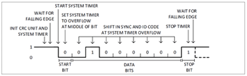
 ; reset timer and set timer limit to middle of bit
 LDI 18, r0
 STS r0, SYSTEM_TIMER, SYSTEM_TIMER_LIMIT_W
 ; wait for falling edge (start bit)
 WAIT0SF WAIT_IN1, WAIT_START_TIMER
 ; wait for middle of start bit
 WAIT1SF WAIT_OVERFLOW_TIMER, WAIT_NO_ACTION
 ; set limit to 100MHz / 39 = 2.5MHz and no timer reset
 LDI 39, r0
 STS r0, SYSTEM_TIMER, SYSTEM_TIMER_LIMIT_NO_RESET_W
 REP 8, 1
 ; wait for timer overflow and shift in sync code 010 and cc0..cc4
 SHRI WAIT1SF WAIT_OVERFLOW_TIMER, FLAG_IN1_CRC, r1 ; CF -> r1
 ; wait for timer overflow, stop bit
 WAIT1SF WAIT_OVERFLOW_TIMER, WAIT_STOP_TIMER
システム・タイマーが設定され、プログラムはエンコーダからDIRECT_IN(1)へ返される応答メッセージのスタート・ビットの立下がりエッジを待って(WAIT0SF)から、直ちにタイマー(WAIT_START_TIMER)を起動します。タイマーは、以前の約半分の時間(制限値が39 ではなく18 に設定されている)でオーバーフローし、スタート・ビットの中央に達するようにプログラムされています。この位置に達すると直ちに制限値が改めて39 に設定され、受信データ・ビットの中央に達するごとにタイマー・オーバーフロー・イベントが生成されるようにします(図9)。次いで、「REP 8, 1」反復コマンドとその後の右シフト・イン・コマンドSHRI を使い、受信データのその後の8 ビットがLSB ファーストでシステム・レジスタr1 にシフト・インされ、同時にCRC 計算のためCRC ユニットにもシフト・インされます。最後のストップ・ビットの中央に達すると、直ちにタイマーが停止します。以上で受信制御フィールド・データがレジスタr1 に格納され、最初に受信した8 ビットのCRC チェックサムが計算されます。

エンコーダから送られてくる2 番目のデータグラムは2 番目のバイトで構成され、これはステータス・フィールド(SF)を含んでいます。この場合もタイマー・オーバーフローはスタート・ビットの中央に設定され、DIRECT_IN(1)で立下がりエッジが検出されると、直ちにタイマーが起動します。
; reset timer and set timer limit to middle of bit
 LDI 18, r0
 STS r0, SYSTEM_TIMER, SYSTEM_TIMER_LIMIT_W
 ; wait for falling edge (start bit)
 WAIT0SF WAIT_IN1, WAIT_START_TIMER
 ; wait for middle of start b
 WAIT1SF WAIT_OVERFLOW_TIMER, WAIT_NO_ACTION
 ; set limit to 100MHz / 39 = 2.5MHz and no timer reset
 LDI 39, r0
 STS r0, SYSTEM_TIMER, SYSTEM_TIMER_LIMIT_NO_RESET_W
 REP 8, 1
 ; wait for timer overflow and shift in dd0..dd3, ea0..ea1, ca0..ca1
 SHRI WAIT1SF WAIT_OVERFLOW_TIMER, FLAG_IN1_CRC, r2 ; SF -> r2
 ; wait for timer overflow, stop bit
 WAIT1SF WAIT_OVERFLOW_TIMER, WAIT_STOP_TIMER
8 個のデータ・ビットは、REP 命令とSHRI 命令の組み合わせを使ってレジスタr2 へシフト・インされ、同時にCRC ユニットにもシフト・インされます。タイマーは、ストップ・ビットの中央に達すると停止します。最後には受信ステータス・フィールドがレジスタr2 に格納されて、8 ビットの制御フィールドと8 ビットのステータス・フィールドに対するCRC チェックサムが計算されます。
次に、1 回転以内における24 ビットのエンコーダ絶対位置が、LSB ファーストで1 バイトずつ3 つのデータグラムに分割されます(ABS0、ABS1、ABS2)。このプログラム・コードの構造は、上に示したステータス・フィールド・データグラム用のコードと非常によく似ています。
; reset timer and set timer limit to middle of bit
 LDI 18, r0
 STS r0, SYSTEM_TIMER, SYSTEM_TIMER_LIMIT_W
 ; wait for falling edge (start bit)
 WAIT0SF WAIT_IN1, WAIT_START_TIMER
 ; wait for middle of start bit
 WAIT1SF WAIT_OVERFLOW_TIMER, WAIT_NO_ACTION
 ; set limit to 100MHz / 39 = 2.5MHz and no timer reset
 LDI 39, r0
 STS r0, SYSTEM_TIMER, SYSTEM_TIMER_LIMIT_NO_RESET_W
 REP 8, 1
 ; wait for timer overflow and shift in d0..d7
 SHRI WAIT1SF WAIT_OVERFLOW_TIMER, FLAG_IN1_CRC, r3 ; ABS0 -> r3
 ; wait for timer overflow, stop bit
 WAIT1SF WAIT_OVERFLOW_TIMER, WAIT_STOP_TIMER
エンコーダ位置は、システム・レジスタr3(ABS0)、r4(ABS1)、およびr5(ABS2)内に保存されます。CRC チェックサムの計算は、これら3 つのバイトもカバーするように継続されます。
ID コード0 に対応するエンコーダからの最終データグラムとして、CRC チェックサムが受信されます。このデータグラムのプログラム・コードも、前述のものと非常によく似ています。
 ; reset timer and set timer limit to middle of bit
 LDI 18, r0
 STS r0, SYSTEM_TIMER, SYSTEM_TIMER_LIMIT_W
 ; wait for falling edge (start bit)
 WAIT0SF WAIT_IN1, WAIT_START_TIMER
 ; wait for middle of start bit
 WAIT1SF WAIT_OVERFLOW_TIMER, WAIT_NO_ACTION
 ; set limit to 100MHz / 39 = 2.5MHz and no timer reset
 LDI 39, r0
 STS r0, SYSTEM_TIMER, SYSTEM_TIMER_LIMIT_NO_RESET_W
 REP 8, 1
 ; wait for timer overflow and shift in rc0..rc7
 SHRI WAIT1SF WAIT_OVERFLOW_TIMER, FLAG_IN1, r6 ; CRC -> r6
 ; wait for timer overflow, stop bit
 WAIT1SF WAIT_OVERFLOW_TIMER, WAIT_STOP_TIMER
この場合は、SHRI コマンドによってレジスタにシフト・インされるビットが同時にCRC ユニットにシフト・インされることはありません(シフト・コマンドSHRI の最後のパラメータとしてFLAG_IN1_CRC ではなくFLAG_IN1 が使われます)。受信したCRC 値は、後でシステム・レジスタr6 に格納されます。
以上で、受信したすべてのデータがシステム・レジスタr1~r6 に格納されます。次のステップとして、接続したマイクロコントローラ/モーション・コントローラによって読み出すことができるように、これらの値がSPI バッファにコピーされます。
 ; copy reply to SPI transmit buffer
 LDI %0001_0000, r0 ; its the ABS value
 ST SPI_BUFFER_3, r0 ; 0x10 -> ABS value
 ST SPI_BUFFER_2, r3 ; ABS0
 ST SPI_BUFFER_1, r4 ; ABS1
 ST SPI_BUFFER_0, r5 ; ABS2
最初の32 ビットSPI データグラムは、下位24 ビットの絶対位置情報と、MSB としての固定値0x10 で構成されます。SPI データグラムの読出し時は、この固定MSB 値を使ってこのデータグラムの内容を明確に識別できます。
 ; copy crc value to SPI transmit buffer
 LDI %0111_0000, r0 ; crc values
 ST SPI_BUFFER_3, r0 ; 7 -> CRC + STATUS Field
 ST SPI_BUFFER_2, r2 ;
 LDS SYSTEM_CRC, SYSTEM_CRC_RESULT0_R, r0
 ST SPI_BUFFER_1, r6 ; CRC received
 REV r0, r0
 ST SPI_BUFFER_0, r0 ; CRC calculated
 JA CMD_LOOP
2 番目の32 ビットSPI データグラムには、CRC システム・ブロックからの計算CRC 値がLSB として含まれています。この計算CRC 値は、「LDS SYSTEM_CRC, SYSTEM_CRC_RESULT0_R, r0」命令を使ってシステム・レジスタr0 にコピーされます。この計算CRC 値のビットは、受信したCRC 値とは逆の順番になります。レジスタ・ビットの順番を逆にするには、「REV r0, r0」命令を使用します。データ転送を正常に行うには、その後のレジスタr0 内の計算CRC チェックサムが、受信CRC と同じでなければなりません。
実際のアプリケーションでは、計算CRC チェックサムと受信CRC チェックサムが比較されます。データグラム/エンコーダ全体でこれらのチェックサムが一致しない場合、その情報は破棄または無視され、例えばエラー・フラグがセットされるなどの処置が取られます。
このサンプル・コードでは、32 ビットSPI データグラムのLSB に計算CRC が格納されて、その隣の上位バイトには受信CRC コードが格納されます。受信ステータス・フィールド(SF)は、そのデータグラムの更に隣の上位バイトにコピーされます。最後にMSB は、そのデータグラムの内容がSPI 出力バッファにコピーされる前に、データグラムの内容を識別するために固定値0x70 に設定されます。
付録
アセンブラ
TMC8100 用サンプル/リファレンス・プログラムの開発および変更には、アセンブラを使用できます。PC ベースのコマンド・ライン・ツールには、パラメータとして、アセンブラ・ソース・コードのファイル名とパス(オプション)を入力する必要があります。入力されたファイル名のファイルが見つからない場合は、入力されたファイル名の末尾に自動的に「.asm」が追加されます。アセンブラは、この入力ファイルから出力ファイルを生成します。


この例では、アセンブリ・ソース・コードが保存された入力ファイルの名前は「tmc8100-eval_abn_demo.asm」です。このファイルから生成される機械語命令(16 ビット)の数は83 で、これは使用可能なプログラム・メモリ(SRAM)の4.1%に相当します。TMC8100 のプログラム・メモリのサイズは2K × 16 ビットであり、対応する命令数は最大で2048 個です。
生成されるデフォルトの出力ファイルは1 つで、ファイル名は入力ファイルと同じですが、拡張子は「.asm」ではなく「.hex」になります。この出力ファイルはIntel 標準16 進ファイル・フォーマットのプログラム・コードが保存されたテキスト・ファイルであり、例えば、TMCL-IDE やサンプル・コードで使用できるPython スクリプトの1 つを使い、TMC8100-EVAL-KIT 上にあるTMC8100 のプログラム・メモリにプログラム・コードをロードします。
アセンブラは、異なるフォーマットと追加的な情報で構成されるその他の出力ファイルを生成するためのフラグも、いくつかサポートしています。


- オプション「-i」:「<filename>.i」というファイルがプリプロセッサからの出力として生成されます。このファイルはアッセンブリ・ソース・ファイルの内容で構成され、すべてのプリプロセッサ・コマンド(# ...)が処理されて(例えば「#include」ファイルの内容がソース・ファイルにマージされる)、すべてのコメント(例えば/* .. */ | // | ;)が削除されます。
- オプション「-l」:アッセンブリ・ソース・コード(コメントとプリプロセッサ・コマンドは含まれない)、追加の命令エンコーディング、およびそれらの命令のプログラム・メモリ・アドレスで構成される「<filename>.log」というファイルが生成されます。
- オプション「-c」:TMC8100 をブートストラップするコントローラ用プログラムの開発を支援するために、C コードで構成される「<filename.c>」というファイルが生成されます。このファイルは、整数の配列と、生成された機械語コードで構成されます。
- オプション「-rom」:3 つの追加ファイルが生成されます。機械語命令が16 進/2 進数値として1 行につき1 つずつリストされた「pelican_bootloader.hex」と「pelican_bootloader.bin」、およびvhdl エンティティ宣言の一部として機械語命令を論理コードの形で示した「pelican_bootloader.vhd」です。
- オプション「-m」:機械語フラグ。様々な実装/命令セットをサポートします(TM02 はTMC8100 をカバー)。
- オプション「-h」:スクリーンショットに示すようなヘルプの表示テスト。
サポートされている構文/コマンド
TMC8100 のデータシートに示すように、現在のところアセンブラはTMC8100 のすべての命令をサポートしています。
プリプロセッサ・コマンド
コメント
プリプロセッサは、その後の処理のために入力ファイルからすべてのコメントを削除します。現在は以下のオプションがサポートされています。
- /* <comment> */ - ブロック・コメント - 複数の行を含めることができます(C 言語型)
- // <comment> - 行の最後までのコメント(C/C++言語型)
- ; <comment> - 行の最後までのコメント
#include
#include "<filename>" — その後の処理のために、<filename>にファイル名とオプション・パスで示されたファイルの内容が、#include プリプロセッサ・ディレクティブの位置に挿入されます。#include ディレクティブがあった行は削除されます。
注:<filename>の周囲に記述できるのは引用符だけです。その他のコマンド/アサインを含めても、それらはその後の処理で削除/無視されるので含めることはできません。
#define
#define <label> [<replacement text>]
プリプロセッサは、ソース・ファイル(および#include ステートメントによってインクルードされたファイル)内にあるこのコマンド後の<label>を、<replacement text>に置き換えます。置き換えテキストとして使われるのは、<label>の後に置かれて1 つ以上のスペースによって分離された、<label>からその行の最後までの文字シーケンスです。コメントと引用符内のテキストだけは自動置き換えから除外されます。ラベルはその後、別の#define を同じ<label>と共に使ってソース・ファイル内で定義し直すことができます。
置き換え文字を指定せずに<label>を定義することも可能です。この場合、置き換え文字はありません。これは、例えば条件付きの#ifdefコマンドや#ifndef コマンドと組み合わせて使用すると便利です。
#ifdef, #ifndef, #else, #endif
#ifdef <label> <code block 1> #else <code block 2> #endif
それ以前に<label>が定義されている場合は<code block 1>の内容が解釈されてアセンブラ出力が生成され、<code block 2>は無視されます。中間ファイル(<filename>.i)には<code block 1>だけが表示され、<code block 2>は表示されません。コード・ブロックには複数行のアセンブラ命令などを含めることができます。<label>が定義されていない場合は、もう1 つのコード・ブロックが解釈されます。
#ifndef <label> <code block 1> #else <code block 2> #endif
それ以前に<label>が定義されている場合は<code block 2>の内容が解釈されてアセンブラ出力が生成され、<code block 1>は無視されます。中間ファイル(<filename>.i)には<code block 2>だけが表示され、<code block 1>は表示されません。コード・ブロックには複数行のアセンブラ命令などを含めることができます。<label>が定義されていない場合は、もう1 つのコード・ブロックが解釈されます。
注:#define <label>の使用前に<label>名を挙げるだけでも十分です。置き換え用のテキスト/値を示す必要はありません。
#else 部分はオプションです。#ifdef ブロックまたは#ifndef ブロックはネストできます。
アセンブラ・コマンド
数値
2 進数、10 進数、16 進数での数値指定を容易にするために、様々なフォーマットがサポートされています。これらを以下に示します。
「0x123..」または「$123..」は16 進数として解釈されます(使用文字:0~9、a~f またはA~F)。
「%1010..」は2 進数として解釈されます(使用文字:0 と1)。読みやすくするために文字「_」を挿入できます(例えば8 ビット数の場合は%1010_0011)。
「123..」は10 進数として解釈されます(使用文字:0-9)
識別子
可読性向上のため、数値に代えて識別子を使用できます。識別子は、文字(a~z / A~Z)または「_」から始める必要があります。その後は数値(0~9)を使用することも可能です。文字名の大文字と小文字は区別されません。
下の例に示すように、識別子には等号を使って値を割り当てることができます。
SPI_BUFFER_0 = $30
識別子に使うべきではない名前もいくつかあります。
- アセンブラ命令 - これには、TMC8100 のデータシートにリストされたすべての名前と、コマンドの条件付き実行を示す「C」から始まる命令名が含まれます。
- 識別子r0~r7 は、使用可能な汎用レジスタを指定するためにレジスタ0~7 として予め定義されています。
- ラベルと識別子を同じ名前にすることはできません。
ラベル
ラベルは、プログラム・メモリ・アドレスのプレースホルダとして使われます。ラベルに値を割り当てる必要はありません。ラベルは、アセンブラがアッセンブリ・ソース・コードを機械語コードに変換する際に最新のプログラム・メモリ・アドレスで初期化されます。
エンドレス・ループの例:
WAIT:
JA WAIT
ラベル名の後の「:」文字に注意してください。アセンブラは、次の命令(この場合はJA WAIT コマンド)のプログラム・メモリ・アドレスで、ラベルWAIT を自動的に初期化します。実際に命令の一部として使われる前にラベルが初期化されるジャンプ・バック(上の例)と、命令によって参照された後にラベルが初期化されるジャンプ・フォワードの両方がサポートされています。