AN-1526: High Speed, Precision, Differential AC-Coupled Drive Circuit for the AD7625 16-Bit, 6 MSPS PulSAR ADC
Circuit Function and Benefits
This application note provides a method to drive an ac-coupled differential input signal to the AD7625, 16-bit, 6 MSPS PulSAR® differential analog-to-digital converter (ADC). This circuit is designed to ensure maximum performance of the AD7625 by providing adequate settling time and low distortion. It uses a buffered common-mode voltage (VCM) output voltage from the AD7625 to set the common-mode level of each amplifier.
Circuit Description
The signal source applied to the AD7625 must be buffered to enable driving the AD7625 switch capacitor front end and to maintain low distortion. The ADA4899-1 used on each input provides the required drive, distortion, and settling time to maximize the performance of the AD7625.
Figure 1 shows that the differential ac-coupled source has signals 180° out of phase with each other, and the voltage swings around ground on each input. In the test setup, an Audio Precision AP2700 series generator was used to generate the differential input signals. Two 10 µF NP0 capacitors are used to couple the signal into the driver circuit. The two ADA4899-1 amplifiers are connected in a unity-gain noninverting configuration (the ADA4899-1 is unity-gain stable) to condition the analog input to the AD7625 inputs, thereby providing sufficient isolation from the converter switched capacitor transients and also setting the correct common-mode input voltage. For the AD7625, the common-mode voltage is half the internal reference voltage, REF/2, where REF = 4.096 V.


The VCM output pin of the AD7625 is a useful function that provides half the reference voltage used internally by the AD7625. This VCM output is buffered with the AD8031 rail-to-rail amplifier, thereby providing a precise common-mode voltage for the analog input amplifiers.
Note that the FEEDBACK pin on the ADA4899-1 is internally connected to its output pin, thereby minimizing parasitic capacitance and inductance. The ADA4899-1 also has an exposed pad for heat dissipation, which is recommended to be electrically connected to the ground plane.
To allow sufficient headroom at the output of the ADA4899-1 op amps, both devices are powered with a +7 V and −5 V supply to ensure the output can go to 4.096 V and 0 V. Because the amplifier and the ADC operate on different supply voltages, protection circuits are recommended at the ADC inputs, as described in the MT-036 Tutorial.
Excellent layout, grounding, and decoupling techniques must be utilized to achieve the desired performance from the circuits discussed in this note (see the MT-031 Tutorial and the MT-101 Tutorial). As a minimum, it is recommended to use a 4-layer printed circuit board (PCB) with one ground plane layer, one power plane layer, and two signal layers. The AD7625 data sheet also includes information on layout and decoupling practices for the device.
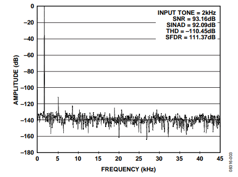
Figure 2 and Figure 3 show the excellent distortion and noise performance obtained with the circuit.


References
MT-036 Tutorial, Op Amp Output Phase-Reversal and Input Over-Voltage Protection, Analog Devices.
MT-074 Tutorial, Differential Drivers for Precision ADCs, Analog Devices.
MT-075 Tutorial, Differential Drivers for High Speed ADCs Overview, Analog Devices.