AN-1268: A Reference Design Using the ADF7241/ADF7242 and Skyworks SE2431L
Introduction
This application note describes a reference design using the Analog Devices, Inc., ADF7241/ADF7242 and the Skyworks Solutions, Inc., SE2431L.
About the ADF7241/ADF7242
The ADF7242 is a highly integrated, low power, and high performance transceiver for operation in the global 2.4 GHz ISM band. It is designed with emphasis on flexibility, robustness, ease of use, and low current consumption. The IC supports the IEEE 802.15.4-2006 2.4 GHz PHY requirements as well as proprietary GFSK/FSK/GMSK/MSK modulation schemes in both packet and data streaming modes. The ADF7241 is a pin-compatible dedicated IEEE 802.15.4-2006 2.4 GHz transceiver.
About the SE2431L
The Skyworks SE2431L is a fully integrated RF front-end module (FEM) designed for 2.4 GHz applications. The SE2431L is designed for ease of use and maximum flexibility, with fully matched 50 Ω input and output, and integrated inter-stage matching, harmonic filter, and digital controls compatible with 1.6 V to 3.6 V CMOS levels.

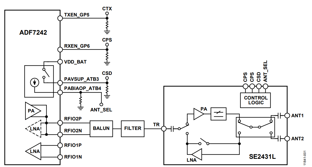
Figure 1. Block Diagram of the ADF7242 on Left Connected to the SE2431L on Right.
General Operation and Performance Data
This section describes the general operating conditions and typical performance realized when using these devices together. Further details regarding the performance of each part are available in the product data sheets.
General Operating Conditions
| Parameter | Min/Max | Unit |
| Supply Voltage Range | 2.0/3.6 | V |
| Frequency Range | 2400/2485 | MHz |
| Temperature Range | −40/+85 | °C |
Typical Performance Data
| Parameter | Typ | Unit | Condition |
| Transmit Power Maximum | 21.5 | dBm | Supply voltage 3.3 V |
| Harmonics 1 | |||
| 2nd Harmonic with +20 dBm Output Power | −54 | dBm | Conducted |
| 3rd Harmonic with +20 dBm Output Power | −50 | dBm | Conducted |
| Receiver Sensitivity | |||
| 50 kbps | −106 | dBm | 10−3 BER FSK (fDEV = 30 kHz) |
| 500 kbps | −100 | dBm | 10−3 BER GFSK (fDEV = 250 kHz) |
| 1 Mbps | −97 | dBm | 10−3 BER GFSK (fDEV = 250 kHz) |
| IEEE 802.15.4 | −100 | dBm | 1% PER |
| Current Consumption | |||
| Rx LNA Bypass Mode | 19.5 | mA | |
| Rx LNA On | 24.4 | mA | |
| Tx Output Power +20 dBm | 150 | mA | |
| Saturation Level 2 | −29 | dBm | 0.1% BER, Rx LNA on |
| 1 Passed FCC Part 15.247 radiated harmonics pre-compliance testing with +20 dBm output power on the ADF7242DB5Z reference design described in this application note. Passed ETSI EN300 328 section 4.3.6 and 4.3.7 radiated spurious emissions pre-compliance tests on the ADF7242DB5Z reference design described in this application note. |
|||
| 2 For input powers approaching or higher than the saturation level, select LNA bypass mode. Note this is the power level at the input to the SE2431L. The RSSI readback will reflect the power seen at the input to the ADF7241/ADF7242; the SE2431L LNA gain should be accounted for. This is nominally 13 dB. | |||
Modes Of Operation
The Skyworks FEM has four modes of operation as outlined in Table 3. The FEM also supports antenna diversity. Table 3 and Table 4 show the control logic for the different modes and for antenna selection, respectively.
| Mode No. | Mode Description | RXEN_GP6 > CPS | PAVSUP_ATB3 > CSD | TXEN_GP5 > CTX |
| 0 | All off (sleep mode) | 0 | 0 | 0 |
| 1 | Rx bypass mode | 0 | 1 | 0 |
| 2 | Rx LNA mode | 1 | 1 | 0 |
| 3 | Tx mode | X | 1 | 1 |
| Mode Description | PABIAOP_ATB4 > ANT_SEL |
| ANT1 Port Enabled | 0 |
| ANT2 Port Enabled | 1 |
Table 3 and Table 4 also show suggested pin connectivity between the ADF7241/ADF7242 and the SE2431L for these controls. In these tables, the pin names on the left are Analog Devices pins and the pin names on the right are Skyworks pins. For example, in the third column of Table 3, the Analog Devices RXEN_GP6 output pin drives the Skyworks CPS input pin.
Switching Between FEM Modes
Using the suggested pin connectivity switching between the modes of the FEM can be controlled through register settings on the ADF7241/ADF7242.
| Register 1 | Mode 0 (All Off) | Mode 1 (Rx Bypass Mode) | Mode 2 (Rx LNA Mode) | Mode 3 (Tx Mode) | |||
| ANT1 | ANT1 | ANT2 | ANT1 | ANT2 | ANT1 | ANT2 | |
| 0x100 | 0x00 2 | 0x08 | 0x08 | 0x18 | 0x18 | 0x18 | 0x18 |
| 0x31E | 0x07 | 0x17 | 0x17 | 0x17 | 0x17 | 0x17 | 0x17 |
| 0x3A9 | 0x14 | 0x14 | 0x14 | 0x14 | 0x14 | 0x14 | 0x14 |
| 0x3AA | 0xF0 | 0xF0 | 0xF1 | 0xF0 | 0xF1 | 0xF0 | 0xF1 |
| 1 When using RXEN and TXEN to control the FEM, Register gp_cfg, Field gpio_config setting 0x7 is not allowed because it also uses RXEN and TXEN. | |||||||
| 2 For Mode 0, Field extpa_auto_en in Register 0x100 must be set to 0. The rxen_en and txen_en fields in Register 0x100 may be regarded as don’t care in this mode. Thus, for example, this register could be left at setting 0x18 in Mode 0. |
|||||||
Transitioning From Mode 0 To Mode 1
ADF7242 Register 0x100, Register 0x3A9, and Register 0x3AA should be programmed in Idle mode. Register 0x31E must be programmed in PHY_RDY mode. The FEM remains in Mode 0 until Register 0x31E is programmed to 0x17; then goes high if the extpa_bias_mode field in Register 0x3AA is set to 0x0 or 0x1. This results in a transition to Mode 1.
Transitioning Between Mode 1 And Mode 2 Or Mode 3
With the rxen_en and txen_en fields in Register 0x100 set high, RXEN and TXEN automatically go high as the transceiver enters Rx or Tx, respectively, and low again when it exits. This supports transitions from Mode 1 to Mode 2 and Mode 3 as well as the automatic return to Mode 1 when the transceiver exits Rx or Tx.
When the rxen_en field in Register 0x100 is set low and the txen_en field is set high, TXEN automatically goes high on entering Tx and returns low on exiting Tx. RXEN remains low. This supports the automatic transition to Mode 3 when the transceiver enters the Tx state and returns to Mode 1 at the end of Tx; however, in this case, the FEM remains in Mode 1 for Rx.
If in Mode 2, to transition to Mode 1 while remaining in Rx, set Register 0x32E to 0x00. To revert back to Mode 2 while in Rx, set Register 0x32E to 0x40.
Transitioning Back To Mode 0
When the transceiver enters Idle state, Register 0x31E automatically resets to 0x00 bringing ATB3/CSD low, putting the FEM into Mode 0. This section provides two examples.
Examples
After configuring the ADF7241/ADF7242 in Idle mode as normal,
- From Idle mode, to enter Rx with the external LNA enabled and using Antenna 1, perform the following SPI writes:
- 0x190018
- 0x1BA914
- 0X1BAAF0
- 0XB3
- 0x1B1E17
- 0xB4
Note that the external LNA is automatically disabled when you exit Rx mode.
- From Idle mode, to enable the external PA when entering Tx and using Antenna 1, perform the following SPI writes:
- 0x190018
- 0x1BA914
- 0X1BAAF0
- 0XB3
- 0x1B1E17
- 0xB5
Note that the external PA is automatically disabled when you exit Tx mode.
Reference Evaluation Board
This section provides a schematic and bill of materials (BOM) for creating your own reference evaluation board to test the reference design described in this application note. Note that this evaluation board was developed to demonstrate capability, performance, and compliance. Analog Devices does not provide this hardware; however, details of the schematic and Bill Of Materials are provided here to support users in their board design. The gerber files of the layout are also provided. Note that users should adhere to best RF practices in their specific implementation.
Schematic

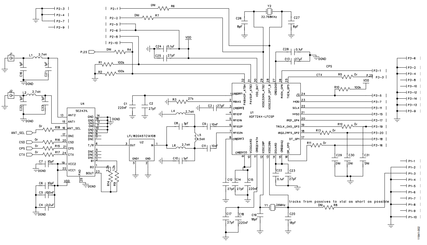
Figure 2. ADF7242 SE2431L Reference Evaluation Board Schematic.
Bill Of Materials
| Qty | Reference Designator | Value | Tolerance | PCB Decal | Manufacturing Part No. |
| 3 | C1, C15, C18 | 220 nF | 10% | 0402 | LMK105BJ224KV-F |
| 8 | C2, C3, C12, C13, C14, C17, C23, C25 | 27 pF | 5% | 0402 | C0402C270J5GACTU |
| 2 | C8, C10 | 1 pF | 10% | 0402 | GRM1555C1H1R0BZ01D |
| 4 | C16, C21, C32, C33 | 1 pF | ±0.25 pF | 0402 | GRM1555C1H1R0CZ01 |
| 2 | C9, C11 | 10 nF | 10% | 0402 | GRM155R71H103KA88D |
| 2 | C19, C20 | 18 pF | 5% | 0402 | GRM1555C1H180JZ01D |
| 4 | C5, C22, C24, C28 | 0.1 µF | 10% | 0402 | GRM155R71C104KA88D |
| 2 | C26, C27 | 8 pF | 0.5 pF | 0402 | GRM1555C1H8R0DZ01D |
| 1 | C4 | 2.2 µF | 10% | 0603 | GRM188R71A225KE15D |
| 2 | C6, C7 | 10 pF | ±0.5 pF | 0402 | GRM1555C1H100JZ01 |
| 3 | L1, L4, L6 | 2.7 nH | 5% | 0402 | Coilcraft 0402CS-2N7X_JLU |
| 1 | L5 | 9.5 nH | 5% | 0402 | Coilcraft 0402CS-9N5X_JLU |
| 3 | R1, R2, R10 | 100 kΩ | 1% | 0402 | RC0402FR-07100KL |
| 1 | R3 | 27 kΩ | 1% | 0402 | MCR01MZPF2702 |
| 7 | R11, R12, R13, R15, R16, R17, R18 | 0 Ω | 1% | 0402 | MCR01MZPJ000 |
| 1 | R9 | 1.2 kΩ | ±5% | 0402 | ERA-2AED122X |
| 1 | R14 | 2.2 kΩ | ±5% | 0402 | ERJ-2GEJ222X |
| 9 | C29, C30, C31, L2, R4, R5, R6, R7, R8 | DNI | Do not insert | ||
| 1 | U1 | 2.45 GHz | 5 mm × 5 mm | ADF7242 | |
| 1 | U2 | 2.45 GHz | 0603 | LFL182G45TC1A208 | |
| 1 | U3 | 2.45 GHz | 3 mm × 4 mm | SE2431L | |
| 1 | Y1 | 26 MHz | 3.20 mm × 2.50 mm | NX3225SA-26.000000MHZ-G2 | |
| 1 | Y2 | 32 KHz | 3.20 mm × 1.50 mm | ABS07-32.768KHZ-7-T |
Note that, alternatively, it is possible to control ANT_SEL from a microcontroller by removing R5 and inserting the 0 Ω link at R4 or by driving the ATB4 pin on the motherboard.
ADF7241/ADF7242 Port Impedance Data For The RF102 RF Port
Note the following port impedance data:
- LNA differential port impedance: 101 −j99.6
- Optimum differential PA load impedance: 87.35 +j70.5
Typical Timing For FEM Control Logic
The following plots show the typical timing information for signals controlling the FEM operation.

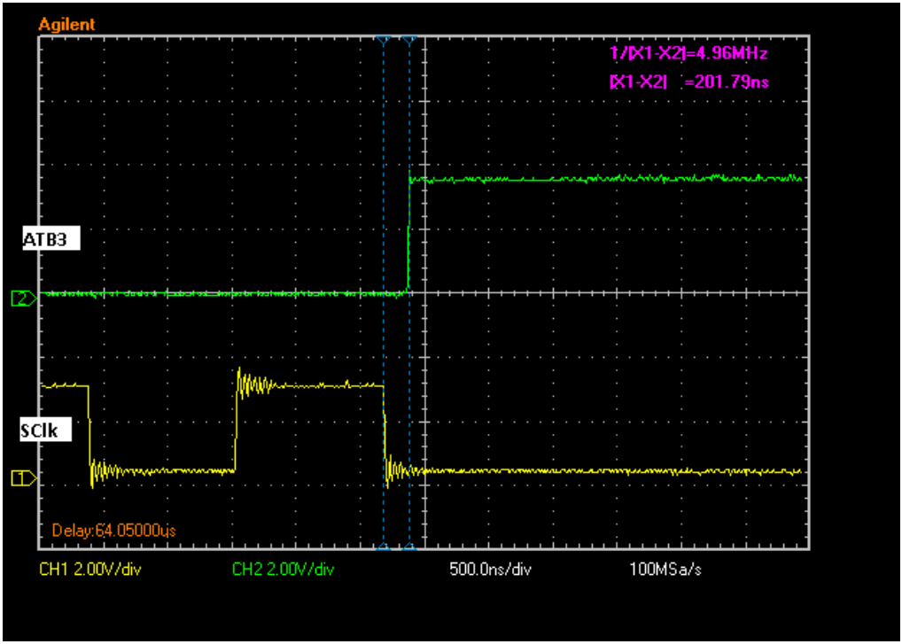
Figure 3. Time from Register 0x31E Register Write (Last SCLK Edge) to ATB3 High (Enabling FEM).

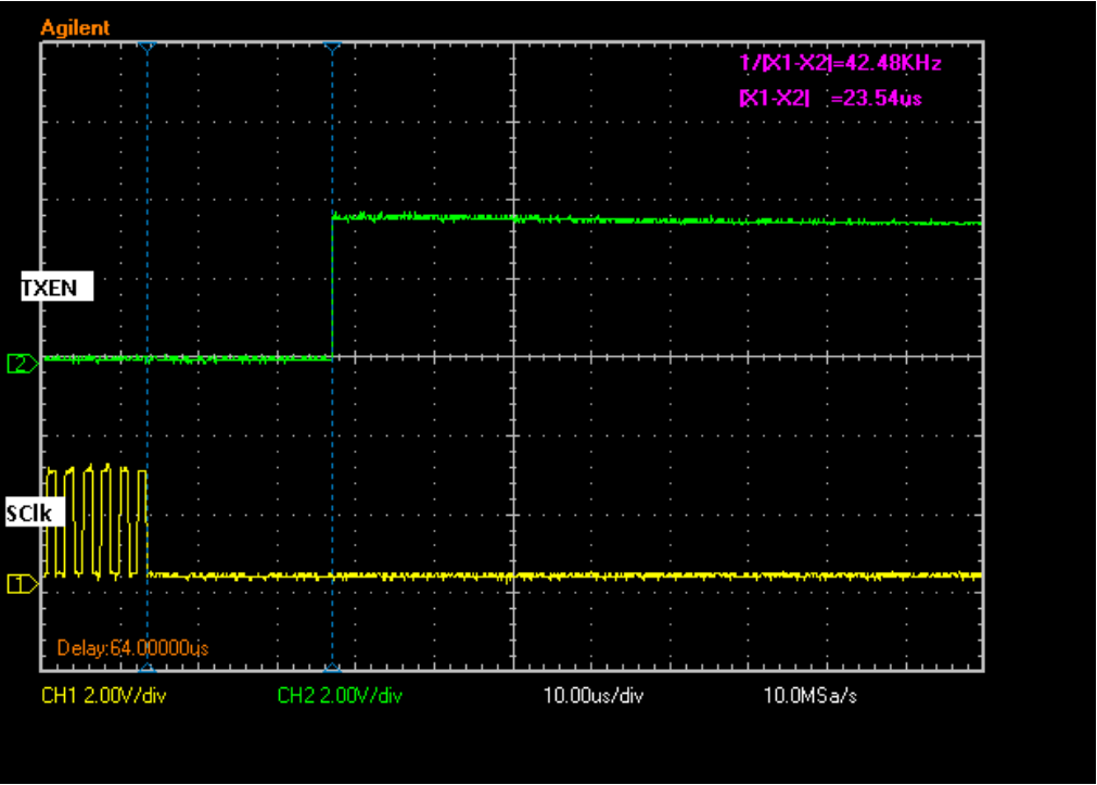
Figure 4. Time from RC_TX Command Write (Last SCLK Edge) to TXEN High.


Figure 5. Time from tx_pkt_sent Interrupt to TXEN Low.

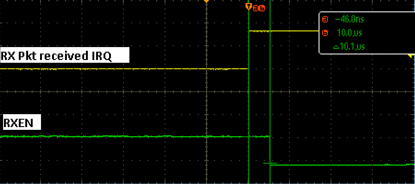
Figure 6. Time from RX Pkt received (rx_pkt_rcvd) Interrupt to RXEN Low.

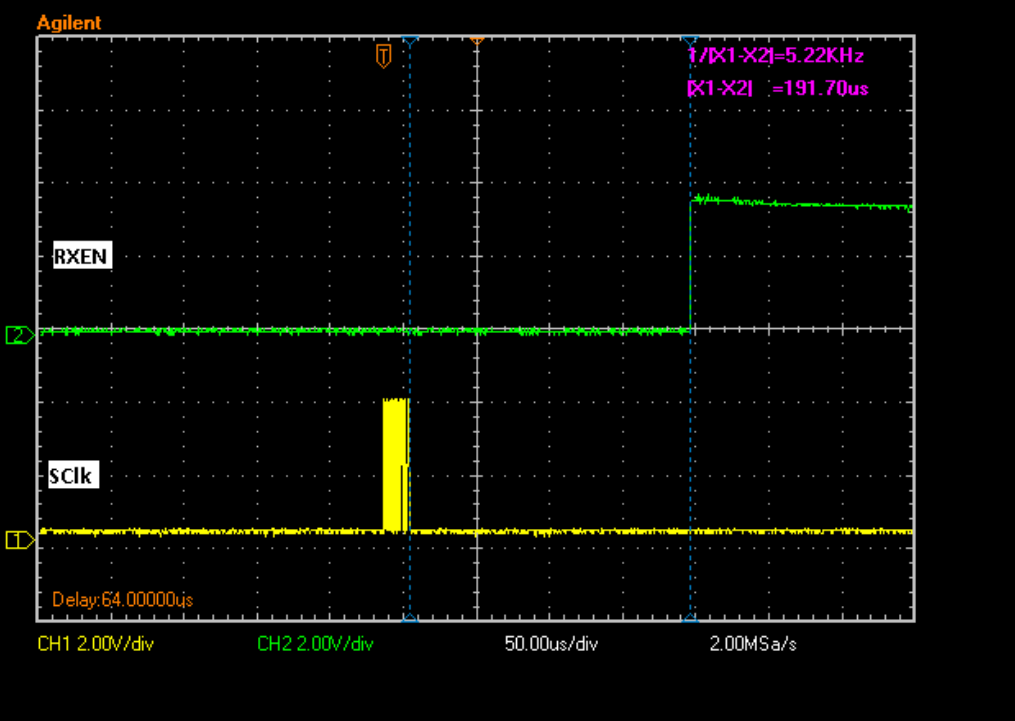
Figure 7. Time from RC_RX Command Write (Last SCLK Edge) to RXEN High with mac_delay timer Set to 192 µs.

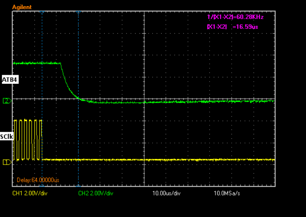
Figure 8. Time from Register 0x3AA Write (Last SCLK Edge) to ATB4 Low (Switching from Antenna Port 2 to Antenna Port 1).

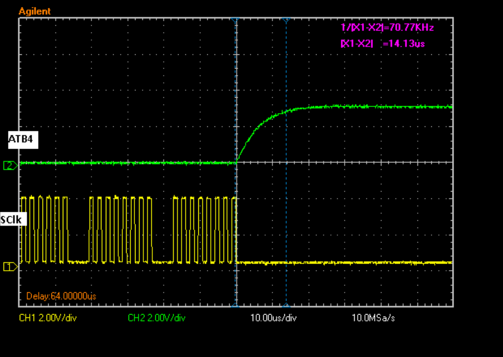
Figure 9. Time from Register 0x3AA Write (Last SCLK Edge) to ATB4 High (Switching from Antenna Port 1 to Antenna Port 2).
著者
