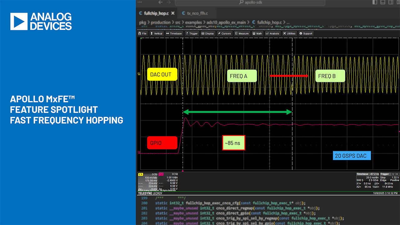
Improve S21 Flatness Measurements
An important performance measure of a 2-port network is S21. A 2-port network can be an amplifier or a filter, for example. So what is S21? This parameter is one of several S-parameters that are commonly used to characterize 2-port networks. An S-parameter indicates the amount of power leaving one port of the network, given power entering another (or the same) port of the network. In the case of S21, the suffix “21” denotes the power leaving port 2, with power delivered to port 1. Note that in the RF world, S-parameters are measured using a 50Ω system. The source impedance driving port 1 must be 50Ω, and the load impedance presented to port 2 must also be 50Ω.
S-Parameters

Suppose the network is an amplifier. Then S21 measures the gain of the amplifier, with port 1 being the input and port 2 being the output. What, then, are the characteristics of a good amplifier? For one thing, flatness of gain over frequency is desirable. When the gain varies over frequency, it is often called ripple. Ripple is evident once S21 is measured over frequency.
There can be issues with the test system that will yield inaccurate results for ripple. These issues appear when the test system, either source or load, does not present a 50Ω impedance to the 2-port network. A typical RF test setup will include a signal source driving port 1 of the DUT through a coaxial cable, with port 2 of the DUT driving the load through another cable. Using this method, there are four interfaces, each one at the end of a transmission line (the coaxial cable). If, for example, the source impedance is not quite 50Ω, some small amount of power will be reflected at the interface between the source and the first coaxial cable. Or perhaps the characteristic impedance of the cable is not quite 50Ω; this will also give rise to a reflection. Some small amount of power loss due to a reflection may not be an issue, especially if we are not terribly concerned about the absolute magnitude of the amplifier gain. The problem is the propagation delay of the cable(s). This delay will give rise to steady-state variations in power delivered across the interface over frequency. The reason is that power reflections, even small ones, will selectively add or subtract from the primary power wave as frequency varies. The result is frequency response ripple. The magnitude of the ripple will depend upon the severity of the impedance mismatch at the interface, and the period of the ripple over frequency will depend upon the length of the cable. Ripple can appear in a measurement of S21 even if the frequency response of the DUT is perfectly flat.
So how do we eliminate measurement system ripple in an S21 test? Short of ensuring that all sources, cables, and loads are perfect 50Ω elements, the best way to do this is add attenuation. The reason is that attenuators are resistive, and generally very close to 50Ω impedance over a broad frequency range. They serve to dampen reflections at the interfaces between elements.
Attenuation comes in the form of 50Ω coaxial pads, and they should be placed at the interfaces between the measurement cables and the DUT. Usually 3dB pads serve well, but 6dB pads can yield better results if there is enough RF power in the system to drive the DUT properly. Note that the test system should be calibrated before the S21 test with the pads in place. The measurement system then automatically takes into account the losses of the attenuators.
About the Authors
Related to this Article