Zero-Drift Operational Amplifier Family in Small-Footprint Packages Features 3μV Maximum DC Offset and 30nV/°C Maximum Drift
Zero-Drift Operational Amplifier Family in Small-Footprint Packages Features 3μV Maximum DC Offset and 30nV/°C Maximum Drift
Nov 1 2000
Introduction
The LTC2050, LTC2051 and LTC2052 are single, dual and quad zero-drift operational amplifiers, available in SOT-23, MS8, and GN16 packages, respectively. The smallest zero-drift op amps available, they occupy minimal board space while providing the lowest input offset (3μV max) and offset drift (30nV/°C max) currently available. In addition, they operate over a wide supply range, from 2.7V to ±5V. They have rail-to-rail outputs that can drive loads as small as 1k to either supply rail and they have an input range from the negative supply to typically less than 1V from the positive supply.
Extended Input Common Mode Range with Uncompromising CMRR
At room temperature, and with the input common mode level at mid-supplies, the parts typically have 0.5μV of input-referred offset and are guaranteed to have less than ±3μV. To ensure this DC accuracy over the common mode input range, the LTC2050/LTC2051/LTC2052 have exceptionally high CMRR over a wide range from the negative supply to typically within 0.9V of the positive rail, as shown in Figure 1. For example, as the input is varied over the entire 5V common mode range, the input-referred offset changes typically by less than 0.4μV. Similar levels of PSRR (typically less than 0.1μV of offset per volt of supply change) and the near zero temperature drift ensure that the offset does not exceed 5μV over the entire supply voltage and commercial temperature range.

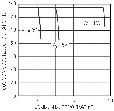
Figure 1. DC CMRR vs input common mode
Rail-to-Rail Output Drive with a 1k Load
The LTC2050/LTC2051/LTC2052 maintain their DC characteristics while driving resistive loads sourcing or sinking currents as high as 5mA. Figure 2 shows the op amps’ rail-to-rail swing versus output resistance loading. With a 1k or 5k load, the output typically swings to within 100mV or 30mV, respectively, of the rails.


Figure 2. Output voltage swing vs load resistance
Clock Feedthrough and Input Bias Current Virtually Eliminated
The LTC2050 family uses autozeroing circuitry to achieve its zero-drift offset and other DC specifications. The clock used for autozeroing is typically 7.5kHz. There are two types of clock feedthrough in autozeroed op amps like the LTC2050/51/52. The first is caused by the settling of the internal sampling capacitor. The input-referred magnitude of this clock feedthrough is independent of input source resistance or gain setting resistors. Figure 3 shows the output spectrum of the LTC2050 with a closed-loop gain of 101 with R2 = 100k, and R1 = RS = 1k. There is a residual clock feedthrough of less than 1μVRMS, input referred, at 7.5kHz. This very low clock feedthrough is achieved in the LTC2050/LTC2051/LTC2052 by internal circuitry that improves settling of the internal autozero storage capacitors.


Figure 3. Output spectrum with a gain of 101; R2 = 100k, R1 = RS = 1k
The second form of clock feed-through is caused by the charge injection of the internal MOS switches connected to the op amp inputs. These current spikes are not evident in the output when the source resistance of the op amp inputs are small (that is, R1 and RS are small in Figure 3). Figure 4 shows the output of the LTC2050HV operating with a gain of 101, 5V supply and the input common mode level at the negative supply (ground). Trace A shows the output when the source resistance (RS) is 1k, whereas trace B shows the output for RS = 100k. The charge injection of the input switches appears in the high input-resistance case. However, the average value of the charge injection current (which is the input bias current) is less than 15pA, as shown in Figure 5. Therefore, even with 100k source resistance, the spikes in Figure 4, trace B can be reduced to 1.5μV input-referred DC with a feedback capacitor across R2.

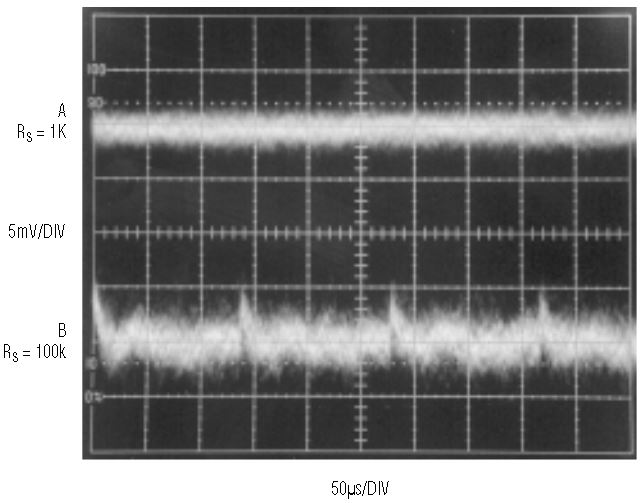
Figure 4. Output with a gain of 101; VS = 5V, R2 = 100kΩ , R1 = 1kΩ , input common mode at V– ; trace A: RS = 1kΩ , trace B: RS = 100kΩ

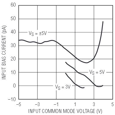
Figure 5. Input bias current vs input common mode voltage (LTC2050HV)
High Resistance Bridge Amplifier Application
A very common application of zero drift amplifiers is amplifying signals from a differential resistive bridge, as shown in Figure 6. The gain is 2R2/R, where R is the bridge resistance. In applications where the bridge resistance is high, input bias current of the op amp can cause errors. With 5V supplies, the LTC2050HV typically has 5pA of input bias current at mid-supply (see Figure 5). Therefore, bridge resistances as high as 100k contribute less than 1μV of additional offset due to input bias current and bridge resistance.


Figure 6. Typical differential bridge amplifier
Ultralow VOS Drift, Low Noise Composite Amplifier
The LTC2050 family of amplifiers has about 1.5μV peak-to-peak noise between DC and 10Hz. If an application needs less noise but requires the LTC2050’s DC performance, a composite amplifier such as the one shown in Figure 7 may be the solution.


Figure 7. Zero drift, low noise composite operational amplifier
The LT1677 is a low noise rail-to-rail input and output op amp that operates over a very wide supply range (3V to ±15V). The integrator formed by the LTC2050HV nulls the offset of the composite amplifier via the offset trim pins of the LT1677. The resulting offset and drift are those of the LTC2050HV but the noise is close to that of the LT1677 (about 100nV peak-to-peak, DC to 10Hz). With the values shown, the warm-up time is about ten seconds.
Negative Supply-Current Monitor
Figure 8 shows the LTC2051 being used to sense the current in the negative power supply. The low offset of the LTC2051 allows the use of a very small sense resistor, RS. The output is level shifted to ground using M1.


Figure 8. Negative supply current monitor
Conclusion
The LTC2050/LTC2051/LTC2052 family of zero-drift operational amplifiers offer smaller packages than any other operational amplifiers with their DC specifications. In addition, they are the first to run on single 2.7V supplies, yet are capable of operation with higher ±5 supplies.
About the Authors


