Single IC Gain Block Provides Accurate Gains from ¼ to 6
In many applications, there is usually a requirement for a gain block either to amplify a weak signal or to attenuate a large signal to match the full-scale input range of an ADC. Unfortunately, typical gain blocks using discrete amplifiers and external resistors have many disadvantages, such as low accuracy and drift limitations. For example, with standard 1%, 100 ppm/°C gain setting resistors, the initial gain error of up to 2% can vary by up to 200 ppm/°C. Generally, one can use precision resistors for precise gain setting, but those can be expensive and occupy a lot of valuable pc board space. Also, the gain can vary with temperature because each resistor drifts differently. Therefore there is a demand for a monolithic amplifier that can provide amplification or attenuation without degrading any performance.
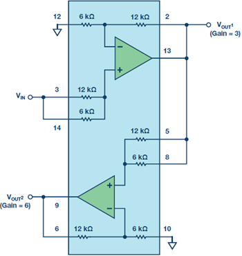
The IC block diagram configurations shown in Figure 1 and Figure 2 offer improved performance at a lower cost, and they are also smaller. This integrated approach is the smallest available for this function and the circuits require no external components.

In Figure 1, the IC is the AD8273, a low distortion, dual-channel amplifier with internal gain setting resistors. With its four trimmed resistors, each channel can be configured as a high performance difference amplifier (G = ½ or 2), inverting amplifier (G = –½ or –2), or noninverting amplifier (G = 1½ or 3). By combining those two amplifiers, one can build a gain block with variable gains of 1/4, 1/2, 1, 2, 3, 4, and 6. The circuit operates on both single and dual supplies and only requires 5 mA maximum supply current.
Although such a circuit can be built discretely, including the resistors on the chip offers advantages to board designers that include better dc specification, better ac specification, and lower production cost. The internal resistors are precisely laser trimmed and tightly matched. Specifications that depend on the resistor matching such as gain drift, common-mode rejection, and gain accuracy are better in this IC than any amplifier design using standard discrete resistors. The integration also improves both board build time and reliability.
The positive and negative input terminals are intentionally not pinned out. Keeping these nodes internal means their capacitance is considerably lower than it would be in discrete designs. Lower capacitance at these nodes means better loop stability and improved common-mode rejection vs. frequency.
With a wide range of supply voltages from ±2.5 V (5 V single-supply) up to ±18 V (36 V single-supply), the circuit is well suited for measuring large industrial signals. Additionally, the part’s resistor divider architecture allows it to measure voltages beyond the supplies.

The companion AD8273 circuit configuration shown in Figure 2 provides an attenuator with the gain of 1/2 or 1/4. The gain block itself comprises two internal difference amplifiers, each with a gain of 0.5. Therefore, the output voltage at VOUT1, providing a precise gain of 1/2 and VOUT2, providing an accurate gain of 1/4.

All resistors are internal in the gain block, so both accuracy and drift are excellent. Typically, these circuits have gain accuracy better than 0.1% with a gain temperature coefficient lower than 5 ppm/°C. Because the circuit is integrated into one chip rather than several discrete components placed on the PCB, the board can be built more quickly and efficiently.
In conclusion, it is easy to see that using a gain block with integrated amplifiers with internal gain setting resistors has many advantages over a discrete amplifier design. Many ICs with resistors on the chip can be connected for a wide range of options. Also, using the on-chip resistors provides the designer with several performance advantages over a discrete design, because most of the dc performance of op amp circuits depend on the accuracy of the surrounding resistors. The internal resistors are laser trimmed and tested for matching accuracy. Therefore, the IC meets many high specifications such as gain drift, common-mode rejection, and gain error. And with its space saving package, it reduces PCB area. In summary, the monolithic gain block simplifies layout, decreases cost, and automatically improves system performance.


