New 333ksps, 16-Bit ADC Offers 90dB SINAD and –100dB THD
The fastest, highest performance 16-bit sampling ADC is now available in a tiny 36-pin SSOP package from Linear Technology. It is the LTC1604. This device runs at 333ksps and delivers excellent DC and AC performance. The LTC1604 operates on ±5V supplies and typically draws only 220mW. It is a complete differential, high speed, low power, 16-bit sampling ADC that requires no external components. The LTC1604 also provides two power shutdown modes, NAP and SLEEP, to reduce power consumption during inactive periods. This 333ksps, 16-bit device not only offers the performance of the best hybrids but also provides low power, small size, an easy-to-use interface and the low cost of a monolithic part. Some of the key features of this new device include:
- 333ksps throughput
- 16 bits with no missing codes and ±2LSB INL
- Low power dissipation and power shutdown
- Excellent AC and DC performance
- Small package—36-pin SSOP
These features of the LTC1604 can simplify, improve, and lower the cost of current data acquisition systems and open up new applications that were not previously possible because no similar part was available.
Fast Architecture
To achieve 333ksps with outstanding AC and DC performance at the 16-bit level, careful design is required. Figure 1, the LTC1604 block diagram, illustrates the design of this part. A high performance differential sample-and-hold circuit, combined with an extremely fast successive-approximation ADC and an on-chip reference, delivers an excellent combination of AC and DC performance. A digital interface allows easy connection to microprocessors, FIFOs or DSPs.
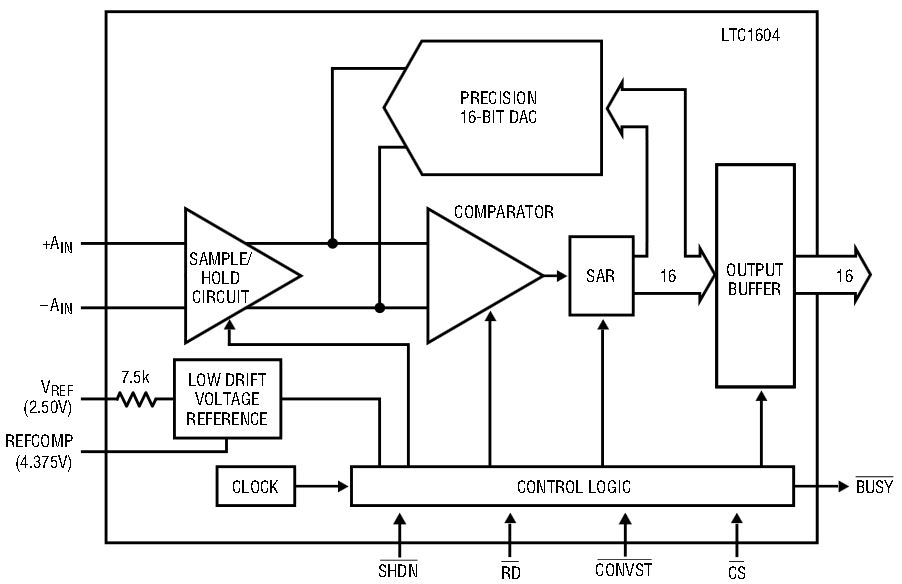
Figure 1. LTC1604 block diagram.
Outstanding AC and DC Performance
The DC specifications include 16 bits with no missing codes and ±2LSB integral nonlinearity error guaranteed over temperature. The gain of the ADC is held nearly constant over temperature with an on-chip 10ppm/°C (typical) curvature-corrected bandgap reference. Figures 2 and 3 show INL and DNL error plots, respectively, for the LTC1604.
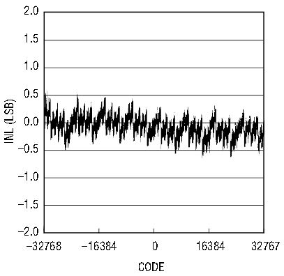
Figure 2. The LTC1604 is very accurate, as shown in the INL error plot. This accuracy is achieved without autocalibration and its associated overhead. Accuracy relies on capacitor matching, which is very stable over temperature and time.
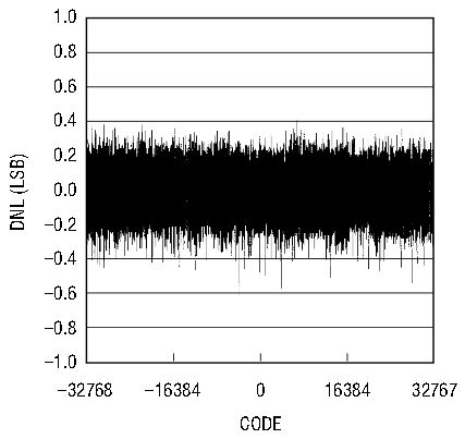
Figure 3. The differential nonlinearity error plot shows the excellent performance of the LTC1604.
The sample-and-hold circuit determines the dynamic performance of the ADC. The LTC1604 has a wide bandwidth, very low distortion, differential sample-and-hold. Fast Fourier transform (FFT) test techniques are used to test the LTC1604’s frequency response, distortion and noise at the rated throughput. By applying a low distortion sine wave and analyzing the digital output using an FFT algorithm, the ADC’s spectral content can be examined for frequencies other than the fundamental. Figures 4 and 5 show the excellent AC performance of the LTC1604 at 333ksps with fIN = 5kHz and 100kHz, respectively. The AC performance of the LTC1604 include total harmonic distortion of –100dB for a 5kHz input and –94dB for a 100kHz input and an input bandwidth of 15MHz for the sample-and-hold.
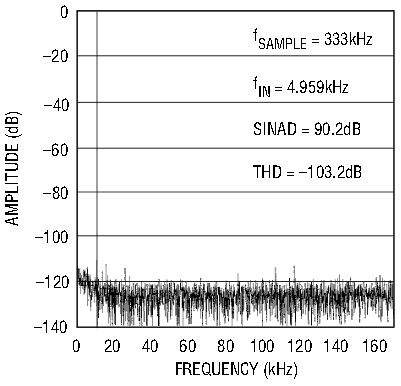
Figure 4. This FFT of the LTC1604’s conversion of a full-scale 5kHz sine wave shows outstanding response with a very low noise floor when sampling at 333ksps.
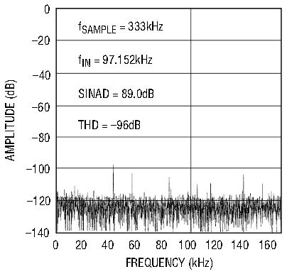
Figure 5. Even with inputs at 100kHz, the LTC1604’s dynamic linearity remains robust.
Very Low Noise
The noise of an ADC can be evaluated in two ways: by signal-to-noise ratio (SNR) in the frequency domain and by histogram in the time domain. The LTC1604 excels in both. Figure 4 demonstrates that the LTC1604 has a SNR of over 90dB in the frequency domain. The noise in the time-domain histogram is the transition noise associated with a high resolution ADC, which can be measured with a fixed DC signal applied to the input of the ADC. The resulting output codes are collected over a large number of conversions. The shape of the distribution of codes will give an indication of the magnitude of the transition noise. In Figure 6, the distribution of output codes is shown for a DC input that has been digitized 4096 times. The distribution is Gaussian and the RMS code transition noise is about 0.66LSB. This corresponds to a noise level of 90.9dB relative to full scale. When added to the theoretical 98dB of quantization error for a 16-bit ADC, this yields an SNR of 90.1dB, which correlates very well with the frequency domain measurements.
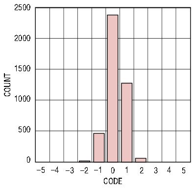
Figure 6. This histogram shows that the LTC1604 has an RMS code transition noise of 0.66dB.
Differential Inputs Ignore Common Mode Noise
Getting a clean signal to the input(s) of an ADC, especially a 16-bit ADC, is not an easy task in many systems. Large noise signals from EMI, the AC power line and digital circuitry are usually present. Filtering and shielding are the common techniques for reducing noise, but these are not always adequate (see “The Care and Feeding of High Performance ADCs: Getting All the Bits You Paid For”; Linear Technology VI:3 [August, 1996]). The LTC1604 offers another tool to fight noise: differential inputs.
Figure 7a depicts a typical single-ended sampling system with ground noise, which may be 60Hz noise, digital clock noise or some other type of noise. When a single-ended input is used, the ground noise adds directly to the input signal. By using the differential inputs of the LTC1604 the ground noise can be rejected by connecting the inputs directly across the signal of interest, as shown in Figure 7b. Ground noise becomes “common mode” and is rejected internally by the LTC1604 by virtue of its excellent common mode rejection ratio (CMRR). Figure 8 shows the CMRR of the LTC1604 versus frequency. Notice that the CMRR is constant over the entire Nyquist bandwidth and is only 6dB lower at 300kHz. This ability to reject high frequency common mode signals is very helpful in sampling systems, where noise often has high frequency components due to switching transients.
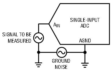
Figure 7a. Single-input ADC measuring a signal riding on common mode noise.
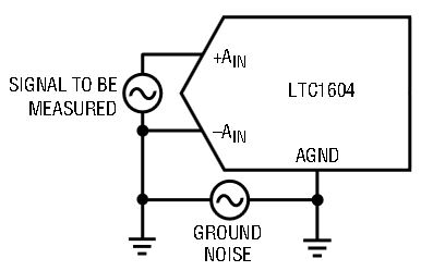
Figure 7b. Differential-input ADC measuring a signal riding on common mode noise.
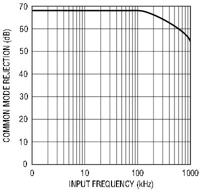
Figure 8. LTC1604 CMRR vs frequency.
3V Input/Output Compatible
The LTC1604 operates on ±5V supplies, which makes the device easy to interface to 5V digital systems. This device can also talk to 3V digital systems: the digital input pins (SHDN, CS, CONVST and RD) of the LTC1604 recognize 3V or 5V inputs. The LTC1604 has a dedicated output supply pin (OVDD) that controls the output swings of the digital output pins (D0–D15, BUSY) and allows the part to talk to either 3V or 5V digital systems.
Low Power Dissipation and Shutdown
The LTC1604 runs at full speed on ±5V supplies and typically draws only 220mW. This power consumption can be reduced further by using the two power shutdown modes, NAP and SLEEP, during inactive periods. NAP mode cuts down the power to 8mW, leaving the reference and logic powered up. The ADC wakes up “instantly” (400ns) from NAP mode, so NAP mode can be invoked even during brief inactive periods with no penalty or delay when conversions must start again.
SLEEP mode is used when there are extended inactive periods. In SLEEP mode, the ADC powers down all the circuitry, leaving the logic outputs in a high impedance state. The only current that remains is junction-leakage current (less than 1µA). It takes much longer for the ADC to wake up from SLEEP mode because the reference circuit must power up and settle to 0.0006% for full accuracy. The wake-up time also depends on the value of the compensation capacitor used on the REF COMP pin. With the recommended 47µF capacitor, the wake-up time is 160ms.
Applications
The performance of the LTC1604 makes it very attractive to use in a wide variety of applications, such as digital signal processing, PC data acquisition cards, medical instrumentation and high resolution or multiplexed data acquisition.
DSP applications often require excellent dynamic performance, since the ADC must sample high frequency AC signals. The LTC1604 is the right choice in these types of applications because of the performance of its sample-and-hold. Figure 9 shows how well the signal-to-noise plus distortion ratio and the spurious free dynamic range of the converter hold up as the input frequency is increased.
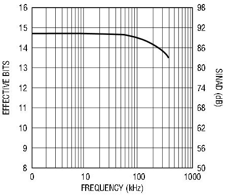
Figure 9. The LTC1604 has essentially flat SINAD and effective bits out to Nyquist.
Another common application is PC data acquisition cards. The high sample rate, the simple, complete configuration and excellent linearity of the LTC1604 make it an ideal choice here. Another advantage that the LTC1604 provides is the synchronized internal conversion clock, which is very useful in this application. This feature eliminates the second external clock required by other sampling ADCs to run conversion, in addition to the normal sample signal. Clearly, this feature makes the LTC1604 an outstanding choice for PC data acquisition cards.
For single-channel or multiplexed high speed data acquisition systems, the LTC1604 has the high sample rate and high impedance inputs that help smooth the design of these applications. High sample rates allow more channels in the data acquisition system on a very low power and cost budget and the high impedance inputs of the ADC make them very easy to multiplex.
Conclusion
The new LTC1604 is a complete 16-bit ADC with a built-in sample-and-hold and reference. It samples at 333ksps and is the fastest device of its kind on the market. The excellent DC and AC performance of the LTC1604 not only make it extremely valuable in a wide variety of existing high resolution applications while also opening up new applications.


