Meeting the Challenges of Power-Supply Design for Modern, High-Current CPUs
Abstract
The performance capabilities of Intel® and AMD® CPUs have increased dramatically over the past five years. This increase in performance has driven an increase in the sophistication and complexity of the voltage regulators that power the CPU. The biggest challenge facing power-supply designers is keeping up with increases in power levels, tighter tolerances, and faster transient requirements, while reducing the overall cost of the power supply. This article explores a brief history of pulse-width modulation (PWM), multiphase operation and current sharing, and some of the latest technological advancements that help designers meet the challenges presented by modern high-power CPUs.
Increasing Performance Requirements and Tightening Cost Constraints
The table below demonstrates how the performance capabilities of CPUs have increased over the past five years. Note the dramatic increase in power requirements, while voltage and in particular voltage tolerances have decreased.
| Features | Pentium® III | Pentium® 4 Extreme |
| Year Introduced | 2000 | 2005 |
| Core Speed (Hz) | 600M | 3.73G |
| L2 Cache | 256K | 2M |
| Front Side Bus Speed (MHz) | 100 | 1066 |
| Voltage (V) | 1.75 | 1.30 |
| Voltage Tolerance (mV) | +40/-80 | ±19 |
| Power (W) | 19.6 | 150 |
- Power One dimension that defines a voltage regulator is the number of 'phases', or channels that it can accommodate. Each phase can practically deliver 25W to 40W of power, depending on factors such as available space and cooling. A single-phase voltage regulator was sufficient for the Pentium 3, while current-generation CPUs require 3- or 4-phase regulators.
- Current Balancing One challenge in designing a multiphase power supply is ensuring that current (power) is properly shared between phases. A significantly disproportionate amount of current in one phase will stress components and degrade their lifetime. Virtually all multiphase voltage regulators incorporate circuitry to actively balance the current between phases.
- Accuracy CPU voltages must be regulated to extremely tight tolerances in order to operate at high clock frequencies. These tight tolerances must be maintained under both static and dynamic load conditions. Static accuracy is achieved through implementation of a precise on-chip reference voltage and through minimization of offset voltages and bias currents. Dynamic accuracy is affected by the control-loop bandwidth of the voltage regulator and the amount of bulk capacitance used on the regulator output. Because no regulator can respond instantaneously to a sudden change in CPU current demand, every design requires bulk capacitance. The higher the regulator control-loop bandwidth, the sooner it can 'catch up' to the CPU's demand and supplement the current provided by the bulk capacitors.
The demands placed on the CPU's voltage regulator are not without cost. Both die area and pin count scale upward with the number of phases that the regulator accommodates. High-accuracy voltage references require sophisticated design and calibration techniques. Amplifiers used for voltage and current sensing, basic voltage regulation, and active current sharing must be designed to be fast with low offset errors and bias currents, and must be stable over process and temperature.
Perhaps the most significant challenge facing high-power CPU regulator designs is cost. Price per phase for a CPU core voltage regulator has declined 4X or more over the past five years.
Basics of Power-Supply Control
Virtually all multiphase voltage regulators use one form of PWM or another. Most are fixed frequency, whereby a clock initiates turn-on of the high-side MOSFET (see QHI in Figure 1) and allows the input supply to charge the inductor.
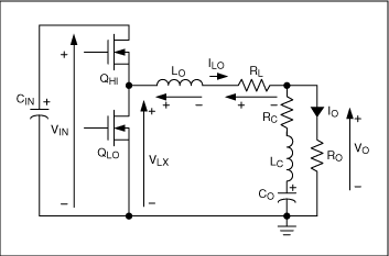
Figure 1. Simplified single-phase buck regulator.
When the control loop determines that it is time to terminate this "on-pulse", the high-side MOSFET is turned off, and the low-side MOSFET is turned on (QLO), allowing the inductor to discharge into the load. This type of PWM control is referred to as trailing-edge modulation, because the leading edge (high-side turn-on) is fixed (by the internal clock) and the trailing edge (high-side turn-off) varies based on the control loop and real-time conditions. The percentage of time that the high-side MOSFET is on relative to the clock period is referred to as the duty cycle (D), and is equal to VOUT/VIN under steady-state conditions.
Voltage mode (see Figure 2) compares the output voltage (or a scaled version thereof) with a fixed internal reference voltage. The result is an error signal that is compared to a fixed internal saw-tooth (or ramp) signal. The ramp signal initiates coincident with the clock pulse, and the output of the PWM comparator remains high as long as the ramp signal is below the error voltage. When the ramp signal crosses through the error voltage, the output of the PWM comparator goes low and the on-pulse is terminated. The voltage loop maintains the output-voltage constant by suitably adjusting the control voltage (VC), and therefore the duty cycle (Figure 3).
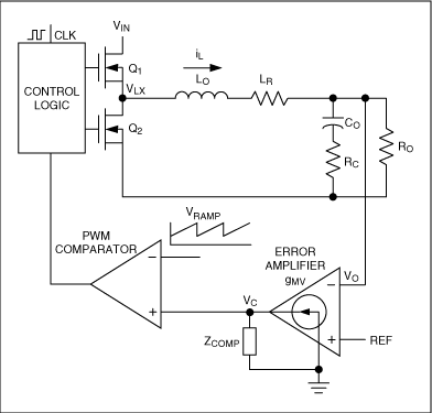
Figure 2. Simplified voltage-mode buck regulator.
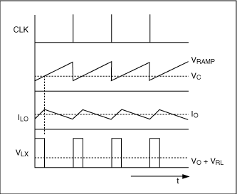
Figure 3. Voltage-mode waveforms.
Peak-current mode (see Figure 4) adds current information to the control loop by replacing the internal ramp used in voltage mode with the ramp generated by the current in the inductor. As with voltage mode, the fixed-frequency clock turns on the high-side MOSFET, causing the inductor current to ramp up. When the (scaled) peak inductor current is equal to the error voltage, the on-pulse is terminated and the high-side MOSFET is turned off. With this approach, there is an outer voltage loop and an inner current loop. The outer voltage loop maintains the output voltage constant by suitably programming the peak inductor current measured by the inner current loop.
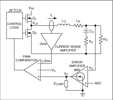
Figure 4. Simplified peak current-mode buck regulator.
Tradeoffs and Considerations
As one would expect, there are pros and cons to each approach. These are discussed in detail in the following paragraphs as they relate to factors that the power-supply designer must consider.
Noise Immunity
Voltage mode has good noise immunity because the magnitude of the ramp signal can be made as large as practical when the control IC is designed. The output voltage is the only sensitive signal routed back to the controller, so voltage mode is relatively easy to layout.
Peak current mode requires that an external current sense signal be routed back in addition to the output voltage. This is done by sensing across a resistance in the load current path (see Current Balancing). To minimize I²R losses, the resistance is kept as small as possible. Therefore, the signal tends to be an order-of-magnitude smaller than the internal ramp generated in voltage mode. Care must be taken to ensure the signal is not corrupted by external noise sources. In practical terms, peak current mode is quite common today, and it is not difficult to lay out using standard good practices.
Line Regulation
Voltage mode inherently responds more slowly to changes in the input voltage. Response to an input voltage change must first be reflected in regulation error of the output voltage, which must be corrected by the voltage-feedback loop. Therefore, response time is limited by the control loop bandwidth. Most contemporary voltage mode regulators do incorporate circuitry to sense the input-voltage change and apply "feed-forward" by adjusting their ramp slope accordingly. However, this adds to the complexity of the controller. Recalling that the duty cycle in peak current mode is controlled by the inductor-current ramp, which is a function of both input and output voltage, we see that peak current mode provides inherent feed-forward on a cycle-by-cycle basis. Therefore, response to line voltage changes is quite fast.
Current Balancing
Voltage regulators composed of two or more phases (multiphase) must actively balance the current between phases to prevent one phase from handling a disproportionate amount of current. Per-phase current sensing can be done by monitoring the current through either the high-side or low-side MOSFET(s), or by sensing the current through a current-sense resistor placed in each phase. The MOSFET methods are inexpensive, as they make use of existing circuit elements, but they are inaccurate because MOSFET resistances vary significantly over process and temperature. The current-sense resistor method can be very accurate, but adds cost and decreases power-supply conversion efficiency.
Another popular method for extracting per-phase current information is to use the DC resistance (DCR) of the inductor as the current-sense element. This approach does not add cost because it makes use of an existing circuit element and provides reasonable accuracy depending on the DCR tolerance. A series resistor and capacitor are added across the inductor, with the RC time constant matched to the L/DCR time constant. The voltage sensed across the capacitor provides a very good DC and AC representation of the current through the inductor. This method is quite commonly used today by both voltage-mode and current-mode CPU regulators.
How voltage mode and current mode use this information brings us to another tradeoff. Because voltage mode only uses voltage information in the control loop, it cannot control the individual phase currents in each inductor, which is a requirement for current balancing. Peak current mode provides natural current sharing because it makes use of the inductor current information as part of the control scheme. Modern multiphase voltage-mode regulators must add a secondary control loop to provide current balancing, which increases IC complexity and brings with it other trade-offs as discussed in Voltage Posititioning and Transient Response.
While peak current mode does provide inherent current sharing, there is one artifact that impacts current-matching accuracy. Because the inductor current peak is controlled, but not also the current valley, any mismatch in inductance between two phases (e.g. due to tolerances) will create inductor current ripple signals with different peak-to-peak magnitudes. This creates a DC mismatch in the current between the two phases, and therefore impacts the accuracy with which the phase currents are balanced.
Analog has addressed this limitation through a technology called Rapid Active Averaging (RA²), which averages out the inductor ripple current at each phase. The RA² circuitry (see Figure 5) "learns" the peak-to-peak ripple current of each phase over 5 to 10 switching cycles, and then biases the peak current signal down by half of the ripple current. Since the peak control point has been moved from the inductor current peak to the DC current point, we still have all of the benefits of peak current mode control, but with very accurate DC current matching. As the RA² circuitry is not part of the current-loop path used for regulation, it does not slow down the transient response. This technology is used in the MAX8809A/MAX8810A core regulators designed for Intel VRD 10.1 (and next-generation VRD) and AMD K8 Socket M2.
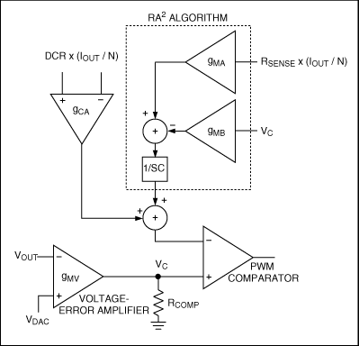
Figure 5. Implementation of RA² Algorithm.
Voltage Positioning and Transient Response
Modern CPUs have large current transients when processor loading suddenly changes. Voltage tolerances must be maintained under these demanding dynamic conditions, otherwise the CPU is prone to lockup. This can be done by ensuring enough bulk capacitance to absorb or supply sudden changes in CPU current; however this adds to overall cost.
Most high-current CPU core-regulator designs use a technique referred to as voltage positioning to reduce bulk capacitance requirements. The output voltage is allowed to decrease (droop) as the load current increases, according to a defined slope. The voltage vs. current line is sometimes referred to as a "load-line", and the slope is specified as impedance (e.g. 1mΩ). The benefit is increased voltage margin under dynamic conditions, which reduces the amount of bulk capacitance required for safe operation.
Ignoring voltage positioning considerations, voltage mode does provide a theoretical advantage in terms of voltage-loop response. Theoretical loop bandwidth is a function of (output-voltage) ripple frequency, or per-phase switching frequency multiplied by the number of phases. With peak current mode, voltage-loop bandwidth is a function of per-phase switching frequency only, due to a phenomena referred to as "sampling effect".
There is a practical difference, however, in voltage positioning applications. Remember that voltage-mode control requires a second control loop for current balancing. The loop bandwidth is generally set to 1/5 to 1/10 of the voltage-loop bandwidth in order to prevent interference with the voltage loop, which is sufficient for current balancing as slow adjustments are usually all that are required. For voltage positioning, however, the ability to respond to a load transient is a direct function of the current-loop bandwidth. For voltage mode, this is quite low (e.g. 5kHz). For peak current mode, the current-loop bandwidth is the same as the voltage-loop bandwidth (e.g. 50kHz to 75kHz) because there is only one loop making use of both voltage and current information. It is quite easy to see the difference this makes in transient performance from the scope shots in Figures 6 and 7. Both show the response to a 95A load step followed by a 95A load release.
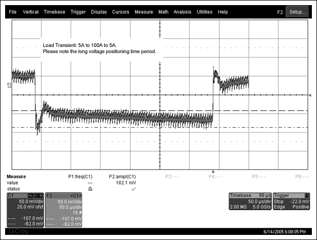
Figure 6. Voltage-mode transient response (competitive product).
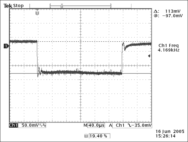
Figure 7. Peak current mode transient response (MAX8810A).
Regulators differ as to how they implement voltage positioning. The secondary current loop present in voltage mode usually provides total average current information. This information, usually a scaled version, is forced through a resistor to set up an offset voltage, which is applied to either the reference (desired output) voltage or the actual (feedback) voltage. The resistor value is selected to provide the appropriate load-line impedance.
The MAX8809A/MAX8810A take a different approach, using finite gain to actively set the output load-line (Figure 8).
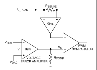
Figure 8. Peak Current Mode Control with Active Voltage Positioning (MAX8810A).
The equation for the error voltage is as follows:
VC = gMV x RCOMP x (VDAC - VOUT)
where gMV is the gain of the error amplifier, RCOMP is a resistor connected between the output of the error amplifier and ground, VDAC is the desired output voltage, and VOUT is the actual output voltage.
Likewise the voltage at the inverting input to the PWM comparator is:
VC = (IOUT / N) x RSENSE x GCA
where IOUT is the output (CPU) load current, N is the number of phases, RSENSE is the value of the current-sense element, and GCA is the current-sense amplifier gain.
In regulation, these two voltages must be equal. With substitution and some rearrangement, we can solve for:
(VDAC - VOUT) / IOUT = (RSENSE x GCA) / (N x gMV x RCOMP)
The term (VDAC - VOUT) / IOUT is what was previously defined as load-line impedance. The current-sense gain (GCA) and the transconductance of the error amplifier (gMV) are constants fixed by the IC design; the parameters RSENSE and N are determined by the application. Therefore, it is easy to program the load-line impedance simply by selecting the proper value of RCOMP, which programs the gain of the voltage-error amplifier.
Loop Compensation
The beauty of the voltage-positioning technique described above for the MAX8809A/MAX8810A lies in its simplicity. The resistor placed at the output of the error amplifier for voltage positioning is also used for loop compensation. Peak current mode only requires single-pole compensation to cancel the zero formed by the bulk capacitors and their ESR. The MAX8809A/MAX8810A only requires the addition of a small-value capacitor parallel to the voltage-positioning resistor. Combination of voltage positioning and loop compensation results in fewer error sources that can impact the regulator's output accuracy.
Voltage-mode control is more complex to compensate due to the poles and zeroes formed by the modulator (control loop) and the output filter. Voltage mode usually requires type III compensation, which increases the number of small resistors and capacitors.
Temperature Compensation
One drawback of using inductor DCR for current sensing is that the DCR changes over temperature according to the positive temperature coefficient of copper. This directly affects the accuracy of both voltage positioning and current-limit protection.
To compensate, designs use a resistor with an equal but opposite (negative) temperature coefficient—an NTC. The NTC is generally part of the resistor network that programs the load-line impedance, which ensures the output voltage vs. current is stable over the operating temperature range. NTCs are not linear over temperature, so the resistor network must include two additional resistors to linearize it over the temperature region of interest.
The drawback is that current-limit information is not temperature-compensated. The current-limit threshold at room temperature must be scaled upward to account for the increased current signal at higher temperatures. At room temperature, the inductor and MOSFETs must be oversized to handle the maximum current at current limit, which in turn leads to a higher solution cost.
Once again, the MAX8809A/MAX8810A provide an example of innovative technology. These regulators also use an NTC, but this information is applied independent of the voltage-positioning circuit. Linearization is integrated, saving two resistors. Temperature-corrected current information is then used internally for both voltage positioning and current limiting. Competing products generally require a second NTC to compensate current limit. The MAX8809A/MAX8810A also use the same internal temperature information for a VRHOT function, a signal indicating that the voltage regulator has exceeded a certain temperature. Thus, three temperature functions are accomplished for the price of one temperature-sensing component, which reduces overall costs.
Conclusion
We have examined the basics of voltage-regulator control, including two popular schemes, voltage mode and peak current mode, used for powering contemporary CPUs. Each approach includes certain tradeoffs that the power-supply designer must consider within the context of a high-current, multiphase design. Features and technology provided by products such as the MAX8809A/MAX8810A core regulators, which implement peak current mode control with RA², help simplify the design process and reduce total solution costs. Please visit Computers: Desktops, Workstations, Servers Overview for complete information on other voltage-regulator solutions for desktop-PC and server applications from Analog.


