Abstract
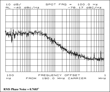
This report provides application data for using the MAX2309 in WCDMA systems with an IF of 190MHz. The MAX2309 offers 110dB gain control range, and operates at 2.7V. MAX2312 in a 28-TSSOP package is compared to the MAX2309 in a 28-pin QFN package. Gain control data, IIP3 data and phase noise data are given. Demodulator phase offest and amplitude data are shown. The IF VGA input impedance is given, along with diagrams showing the test setups.
This report provides application data for using the MAX2309 in a WCDMA receive-path application at 190MHz IF.
General Description of the MAX2309
The MAX2309 is an IF quadrature demodulator designed for CDMA and WCDMA cellular-phone handsets. The signal path consists of a variable-gain amplifier (VGA) and an I/Q demodulator. The devices feature guaranteed +2.7V operation, a built-in VCO and PLL synthesizer, a variable-gain range of over 110dB, and a high IF input dynamic range (-33dBm IIP3 at 35dB gain, +1.7dBm IIP3 at -5dB gain).
The MAX2309 is a member of the MAX2310 series of single-IF and dual-IF demodulators. It is built into a 28-QFN (5x5mm) package and uses the same die as its predecessor, the MAX2312, which comes in a 28-TSSOP package. The baseband, RF, and IF performance have been determined to be identical between the two packages.
The MAX2309/2312 IF LO synthesizer's reference and RF dividers are fully programmable through a 3-wire serial bus, enabling system architectures using any common reference and IF frequency. The differential baseband I-&-Q outputs have enough bandwidth to suit both narrowband and wideband CDMA systems, and offer output levels up to 2.5Vp-p with 2.75V supply voltage.
The MAX2309 Compared to the MAX2312
The MAX2309 and the MAX2312 share the same die, so their operating functions and characteristics are the same. The parasitic packaging change from the original TSSOP-28 to the MAX2309 in the 28-pin QFN was examined carefully, but no net difference to the VCO tuning tank, IF input impedance, or common-mode isolation was found. This is largely because the practical value of VCO tank components and IF input match components are much greater than the lead-frame and bond-wire parasitics. The associated parasitic reactances are virtually unchanged between the two packages (roughly 1nH/0.5pF per lead) and have minimal circuit impact. The smaller package saves board space by as much as 50%.
The MAX2309 Pinout
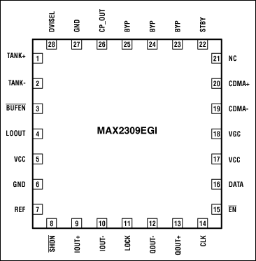
Measured Performance of the MAX2309
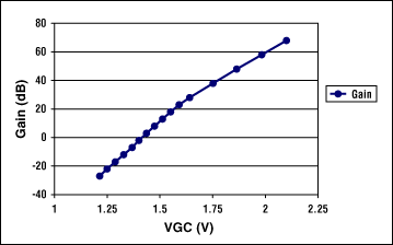
Most of the measurements that were taken were done with the MAX2312. The MAX2309 didn't have its own EV board at the time of the writing, so key electrical operating characteristics were confirmed on Maxim's CDMA Reference Design V2.0, where it has been employed using a 183.6MHz IF. The measurements were driven by a combination of system issues and certain application-specific parameters.
| Pin (dBm) | Vin_RMS (mV) | Vagc (V) | Differential Vop-p (Q) (mV) |
Gain (dB) |
| -5 | 397.63536 | 1.21400 | 50 | -27.04 |
| -10 | 223.60680 | 1.24900 | 50 | -22.04 |
| -15 | 125.74334 | 1.28800 | 50 | -17.04 |
| -20 | 70.71068 | 1.32800 | 50 | -12.04 |
| -25 | 39.76354 | 1.36800 | 50 | -7.04 |
| -30 | 22.36068 | 1.40000 | 50 | -2.04 |
| -35 | 12.57433 | 1.43600 | 50 | 2.96 |
| -40 | 7.07107 | 1.47400 | 50 | 7.96 |
| -45 | 3.97635 | 1.51200 | 50 | 12.96 |
| -50 | 2.23607 | 1.55000 | 50 | 17.96 |
| -55 | 1.25743 | 1.59100 | 50 | 22.96 |
| -60 | 0.70711 | 1.64100 | 50 | 27.96 |
| -70 | 0.22361 | 1.75200 | 50 | 37.96 |
| -80 | 0.07071 | 1.86400 | 50 | 47.96 |
| -90 | 0.02236 | 1.98300 | 50 | 57.96 |
| -100 | 0.00707 | 2.10000 | 50 | 67.96 |
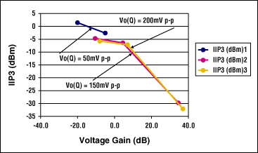
| Pin/Tone (dBm) | Pin Total (dBm) | Vin_RMS (mV) | Vagc (V) | Differential Vop-p (Q) (mV) |
Gain (dB) | IIP3 (dBm) |
| -15 | -12.0 | 177.6172 | 1.246 | 50 | -20.04 | 1.45 |
| -30 | -27.0 | 31.5853 | 1.355 | 50 | -5.04 | -2.6 |
| -15 | -12.0 | 177.6172 | 1.327 | 150 | -10.50 | -4.67 |
| -30 | -27.0 | 31.5853 | 1.43 | 150 | 4.50 | -6.4 |
| -60 | -57 | 0.9988 | 1.684 | 150 | 34.5 | -29.73 |
| -15 | -12 | 177.6172 | 1.348 | 200 | -8 | -5.75 |
| -30 | -27 | 31.5853 | 1.444 | 200 | 7 | -7.08 |
| -60 | -57 | 0.9988 | 1.713 | 200 | 37 | -32.08 |
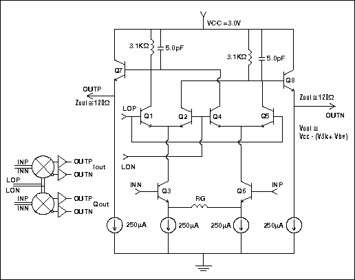
Baseband I-and-Q Output Circuit
The MAX2309/MAX2312 use a traditional Gilbert cell with emitter-follower output buffers for differential baseband I-and-Q outputs. Figure 6 identifies OUTN and OUTP for the differential output pins driven by Q8 and Q7. Also, observe that INN and INP are internal differential inputs from the variable-gain IF amplifier and that LON and LOP are internal differential local oscillator inputs from the on-chip IF VCO.
With VCC at approximately 3.0VDC, the quiescent output voltage at Q7 and Q8 is set by the 250µA bias current through the 3.1kΩ collector loads (around a 0.75-volts drop), summed with the Vbe drop (around 0.7 volts).
Output DC source capability should be around 7mA to 10mA shorted to ground, and sink is around 250µA pulled to VCC. Each pin output resistance should be around 120Ωs, resulting in approximately 240Ω differential drive impedance.
Using Figure 6, note the following tolerance data:
The general value of VOUT:
At any of the I or Q outputs, with VCC = 2.85, unloaded, you should measure around 1.35VOUT DC, which is due to the drop from VCC of 0.77 volts across the 3.1k collector loads plus the Q7/8Vbe of around 0.73-volts DC.
VOUT unloaded varies by:
- ±60mV over process variations, at constant 25°C
- ±90mV over temperature range, given the nominal process
- ±150mV over all temperature plus process variations (that is, worst-caseboundary "corners")
The variation in the output 250µA current sources (more properly called "sinks"):
- 204µA to 317µA over process variations, at constant 25°C
- 168µA to 350µA over temperature range, given the nominal process
- 138µA to 459µA over all temperature plus process variations (that is, worst-case boundary "corners")

| Frequency (MHz) | I-&-Q Phase Offset Phase (deg) | I-&-Q Phase |?| from 90 deg (deg) | I-&-Q Amplitude Imbalance (dB) |
| 185.0 | 89.93 | 0.07 | 0.12 |
| 186.0 | 90.20 | 0.20 | 0.08 |
| 187.0 | 90.45 | 0.45 | 0.09 |
| 188.0 | 90.24 | 0.24 | 0.09 |
| 189.0 | 90.14 | 0.14 | 0.09 |
| 189.9 | 90.26 | 0.26 | 0.13 |
| 190.1 | 89.80 | 0.20 | 0.20 |
| 191.0 | 90.20 | 0.20 | 0.04 |
| 192.0 | 90.40 | 0.40 | 0.09 |
| 193.0 | 90.40 | 0.40 | 0.10 |
| 194.0 | 90.46 | 0.46 | 0.09 |
| 195.0 | 90.72 | 0.72 | 0.13 |
Approximate Model of the Input Impedance Zin
The input impedance of the IF VGA is challenging to measure using a 50Ω S-parameter test set because of its high impedance. The intended operation uses an external parallel resistor across the differential input, forming a broadband IF match. For SAW filters, this typically is 300Ωs to 600Ωs. It was determined experimentally that the equivalent [Rpar || Cpar] input network for low and medium IF have the following approximate values:
| IF Frequency (MHz) | Rin Parallel (kΩ) | Cin Parallel (pF) |
| 85 | 2.02 | 0.45 |
| 90 | 2.09 | 0.42 |
| 95 | 2.08 | 0.44 |
| 100 | 2.00 | 0.42 |
| 105 | 2.10 | 0.42 |
| 110 | 1.98 | 0.42 |
| 115 | 2.10 | 0.39 |
| 120 | 2.01 | 0.42 |
| 125 | 1.98 | 0.39 |
| 130 | 1.95 | 0.40 |
| 135 | 1.91 | 0.39 |
| 140 | 2.00 | 0.41 |
| 145 | 1.95 | 0.38 |
| 150 | 2.02 | 0.40 |
| 155 | 2.01 | 0.38 |
| 160 | 2.03 | 0.38 |
| 165 | 1.97 | 0.39 |
| 170 | 1.85 | 0.39 |
| 175 | 2.06 | 0.39 |
| 180 | 2.02 | 0.41 |
| 185 | 1.93 | 0.40 |
| 190 | 1.95 | 0.38 |
| 195 | 1.93 | 0.42 |
| 200 | 1.95 | 0.40 |
| 205 | 1.88 | 0.41 |
| 210 | 1.99 | 0.39 |
| 215 | 1.92 | 0.41 |
| 220 | 1.98 | 0.42 |
| 225 | 1.93 | 0.41 |
| 230 | 1.82 | 0.40 |
| 235 | 1.95 | 0.40 |
| 240 | 1.79 | 0.42 |
| 245 | 1.83 | 0.42 |
| 250 | 1.81 | 0.42 |
| 255 | 1.78 | 0.42 |
| 260 | 1.85 | 0.41 |
| 265 | 1.89 | 0.43 |
| 270 | 1.84 | 0.42 |
| 275 | 1.78 | 0.42 |
| 280 | 1.84 | 0.44 |
| 285 | 1.84 | 0.43 |
| 290 | 1.76 | 0.42 |
| 295 | 1.72 | 0.44 |
| 300 | 1.89 | 0.43 |
Measurement Setup
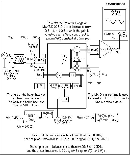
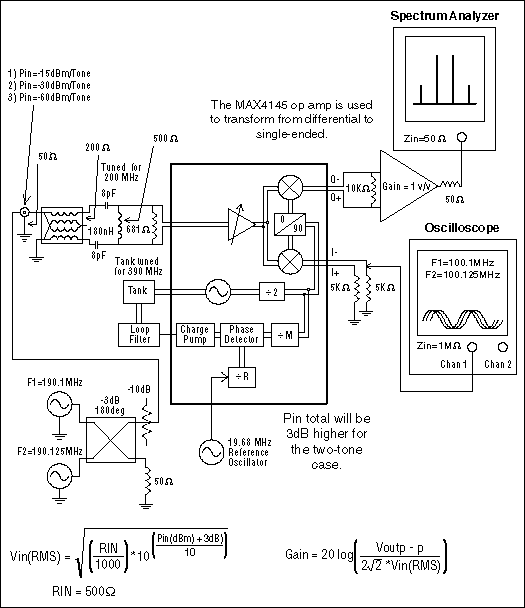
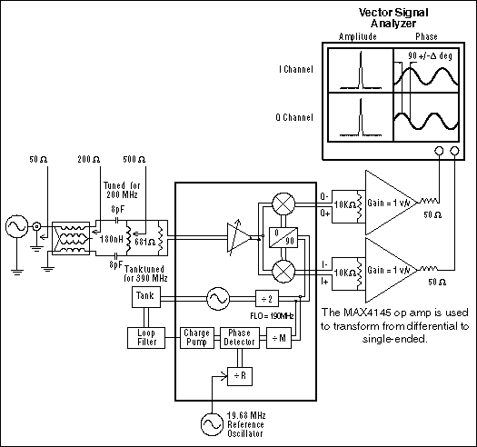
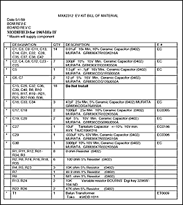
Larger Image (PDF, 12K)
Related to this Article
Products
CDMA IF VGAs and I/Q Demodulators with VCO and Synthesizer
CDMA IF VGAs and I/Q Demodulators with VCO and Synthesizer


