LTC1627 Monolithic Synchronous Step-Down Regulator Maximizes Single or Dual Li-Ion Battery Life
LTC1627 Monolithic Synchronous Step-Down Regulator Maximizes Single or Dual Li-Ion Battery Life
by
Jaime Tseng
Aug 1 1998
Introduction
The LTC1627 is a new addition to a growing family of power management products optimized for Li-Ion batteries. Li-Ion batteries, with their high energy density, are becoming the chemistry of choice for many handheld products. As the demand for longer battery operating time continues to increase and the operating voltages of submicron DSPs and microcontrollers decreases, more demands are placed on DC/DC conversion. The LTC1627 monolithic, current mode synchronous buck regulator (Figure 1) was specifically designed to meet these demands.
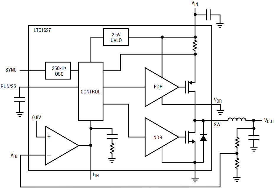
Figure 1. LTC1627 block diagram.
Single and Double Li-Ion Cell Operation
The LTC1627, with its operating supply range of 2.65V to 8.5V, can operate from one or two Li-Ion batteries as well as 3- to 6-cell NiCd and NiMH battery packs. Figure 2 shows a typical discharge voltage profile of a single Li-Ion battery. As shown, a fully charged single-cell Li-Ion battery begins the discharge cycle around 4V (it may be slightly higher or lower, depending upon the manufacturer’s charge-voltage specifications). During the bulk of the discharge time, the cell produces between 3.5V and 4.0V. Finally, towards the end of discharge, the cell voltage drops quickly below 3V. When the voltage drops further, the discharge must be terminated to prevent damage to the battery. A precision undervoltage lockout circuit trips when the LTC1627’s supply voltage dips below 2.5V, shutting the part down to only 5µA of supply current.
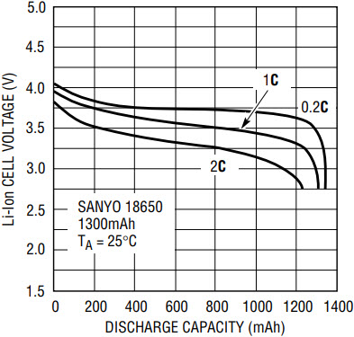
Figure 2. Typical single-cell Li-Ion discharge curve.
Maximizing Battery Run Time
The LTC1627 incorporates power saving Burst Mode operation and 100% duty cycle for low dropout to maximize the battery operating time. In Burst Mode operation, both power MOSFETs are turned off for increasing intervals as the load current drops. Along with the gate-charge savings, unused circuitry is shut down between burst intervals, reducing the quiescent current to 200µA. This extends operating efficiencies exceeding 90% to over two decades of output load range (see Figure 3). As the battery discharges, the LTC1627 smoothly shifts from a high efficiency switch-mode DC/DC regulator to a low dropout (100% duty cycle) switch. In this mode, the voltage drop between the battery input and the regulator output is determined by the load current, the series resistance of the internal P-channel power MOSFET and the inductor resistance.
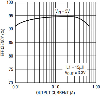
Figure 3. Efficiency vs output load current.
The internal power MOSFET switches provide very low resistance even at low supply voltages. Figure 4 is a graph of switch resistance vs supply voltage for both switches. The RDS(ON) is typically 0.5Ω at 5V and only rises to approximately 0.65Ω at 3V, for both switches. This low switch RDS(ON) ensures high efficiency switching as well as low dropout DC characteristics at low supply voltages.
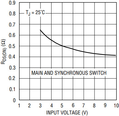
Figure 4. RDS(ON) for both switches vs input voltage.
Extending Low Supply Operation
At low supply voltages, the LTC1627 is most likely to be running at high duty cycles or in dropout, where the P-channel main switch is on continuously. Hence, the I2R loss is due mainly to the RDS(ON) of the P-channel MOSFET. When VIN is below 4.5V, the RDS(ON) of the P-channel MOSFET can be lowered further by driving its gate below ground. The top P-channel MOSFET driver makes use of a floating return pin, VDR, to allow biasing below GND. A simple charge pump bootstrapped to the SW pin realizes a negative voltage at the VDR pin, as shown in Figure 5. Each time the SW node cycles from low to high and then from high to low, charge is transferred from C2 to C1 producing a negative voltage at VDR equal in magnitude to VIN – (2 • VDIODE). In dropout, when the P-channel MOSFET is turned on continuously, a dropout detector counts the number of oscillator cycles that the P-channel MOSFET remains on and periodically forces a brief off period to allow C1 to recharge. When 100% duty cycle is desired, VDR can be grounded to disable the dropout detector.
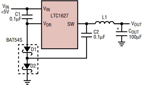
Figure 5. Using a charge pump to bias VDR.
Constant-Frequency, Current Mode Architecture
The LTC1627 uses a constant-frequency, current mode step-down architecture that provides excellent rejection of input line and output load transients and also provides cycle-by-cycle current limiting. Input line transients are rejected by the feed-forward characteristics inherent in current mode control. The output load transients are rejected by the greater error-amplifier bandwidth afforded in current mode control. In current mode, the circuit behaves as if there were a constant current feeding the parallel combination of the output capacitor and output load, yielding only a 90° rather than a 180° phase lag. This simplifies the feedback-loop design and the circuitry around the error amplifier required for stabilization.
Current mode limits the peak current cycle-by-cycle, protecting the internal main switch and synchronous rectifier. In extreme cases, when the output is shorted to ground, the frequency of the oscillator is reduced to one-tenth of its nominal frequency to allow the inductor current time to decay and prevent inductor-current runaway. The oscillator’s frequency gradually increases back to its nominal frequency when VFB rises above 0.3V.
The internal oscillator is set for a fixed switching frequency of 350kHz, allowing the use of small surface mount inductors. In switching-noise-sensitive applications, the LTC1627 can be externally synchronized to frequencies of up to 525kHz. During synchronization, Burst Mode operation is inhibited and pulse-skipping mode is used. In this mode, when the output load is very low, the current comparator remains tripped for more than one cycle and forces the main switch to stay off for the same number of cycles. Increasing the output load slightly allows constant frequency PWM operation to resume.
Minimal External Components
Size is extremely important in modern portable electronics, so the LTC1627 is designed to work with a minimum number of external components. The loop compensation, current sense resistor and the main and synchronous switches are internal. An internal catch diode is also provided across the internal synchronous switch, eliminating parasitic currents or latch-up if the external Schottky diode is omitted. Only an inductor, input and output filter capacitors and two small resistors and capacitors are needed to construct a high efficiency DC/DC switching regulator (see Figure 7). The 47pF filter capacitor connected to the ITH pin (error-amplifier output) filters out switching noise. If the loop compensation needs to be adjusted for a specific application, the ITH pin can also be used for external compensation.
Auxiliary-Winding Control Using the SYNC/FCB Pin
Besides higher efficiency and lower switching noise, synchronous switching provides a means of regulating a secondary flyback winding. In non-synchronous regulators, power must be drawn from the inductor primary winding in order to extract power from auxiliary windings. But with continuous synchronous operation, power can be drawn from the auxiliary windings without regard to the primary output load.
The LTC1627, with its synchronous switching and attendant circuitry, provides the means of easily constructing a secondary flyback regulator, as shown in Figure 6. This flyback regulator is regulated by the secondary feedback resistive divider tied to the SYNC/FCB pin. This pin forces continuous operation whenever it drops below its ground-referenced threshold of 0.8V. Power can then be drawn from the secondary flyback regulator whether the main output is loaded or not.
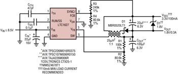
Figure 6. Dual-output 1.8V/0.3A and 3.3V/100mA application.
Typical Applications
1 or 2 Li-Ion Step-Down Converter
Figure 7 is a schematic diagram showing the LTC1627 being powered by one or two Li-Ion batteries. All the components shown in this schematic are surface mount and have been selected to minimize the board space and height. The output voltage is set at 3.3V, but is easily programmed to other voltages.
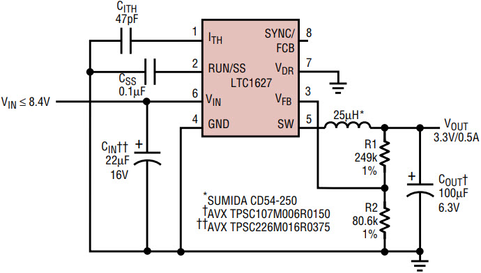
Figure 7. Dual lithium-ion to 3.3V/0.5A regulator.
Single Li-Ion Step-Down Converter
The circuit in Figure 8 is intended for input voltages below 4.5V, making it ideal for single Li-Ion battery applications. Diodes D1 and D2 and capacitors C1 and C2 comprise the bootstrapped charge pump to realize a negative supply at the VDR pin, the return pin for the top P-channel MOSFET driver. This allows Figure 8’s circuit to maintain low switch RDS(ON) all the way down to the UVLO trip voltage.
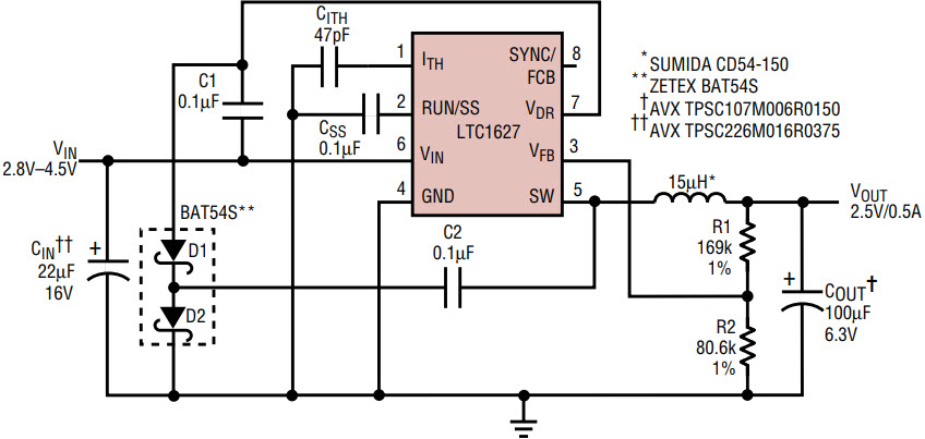
Figure 8. Single lithium-ion to 2.5V/0.5A regulator.
Conclusion
The new LTC1627 monolithic synchronous buck regulator is a versatile, high efficiency, DC/DC converter that is at home in a wide range of low input voltage applications. Features such as precision UVLO and optional bootstrapped gate drive make it particularly well suited to single-cell Li-Ion power.


