LT3420 Charges Photoflash Capacitors Quickly and Efficiently While Using Minimal Board Space
LT3420 Charges Photoflash Capacitors Quickly and Efficiently While Using Minimal Board Space
by
Albert Wu
May 1 2002
Introduction
The LT3420 is a power IC, designed primarily for charging large-valued capacitors to high voltages, such as those used for the strobe flashes of digital and film cameras. These capacitors are generally referred to as photoflash or strobe capacitors and range from values of a hundred microfarads to a millifarad, with target output voltages above 300V. The photoflash capacitor is used to store a large amount of energy, which can be released nearly instantaneously to power a xenon bulb, providing the light necessary for flash photography. Traditional solutions for charging the photoflash capacitor, such as the self-oscillating type, are extremely inefficient. More modern techniques use numerous discrete devices to implement a flyback converter but require a large board area and suffer from high peak currents, reducing battery life. The LT3420 incorporates a low resistance integrated switch and utilizes a new patent-pending control technique to solve this difficult high voltage power problem. Using the LT3420, only a few external components are necessary to create a complete solution, which saves valuable board space in ever shrinking camera designs. Efficiency of the LT3420 is high, typically greater than 75%, while the peak current of the part is well controlled, important features for increasing battery life.
Overview
Figure 1a shows a photoflash application for the LT3420. To generate the high output voltage required, the LT3420 is designed to operate in a flyback switching regulator topology. The LT3420 uses an adaptive on-time/off-time control scheme resulting in excellent efficiency and precise control of switching currents. The LT3420 can charge a 220μF capacitor from 50V to 320V in 3.5s from a 5V input, as shown in Figure 1b. Charge time decreases with higher VIN, as shown in Figure 1c. 50V is used as the starting point in calculating charge time since the xenon bulb will self extinguish at this voltage, halting any further voltage drop on the photoflash capacitor.
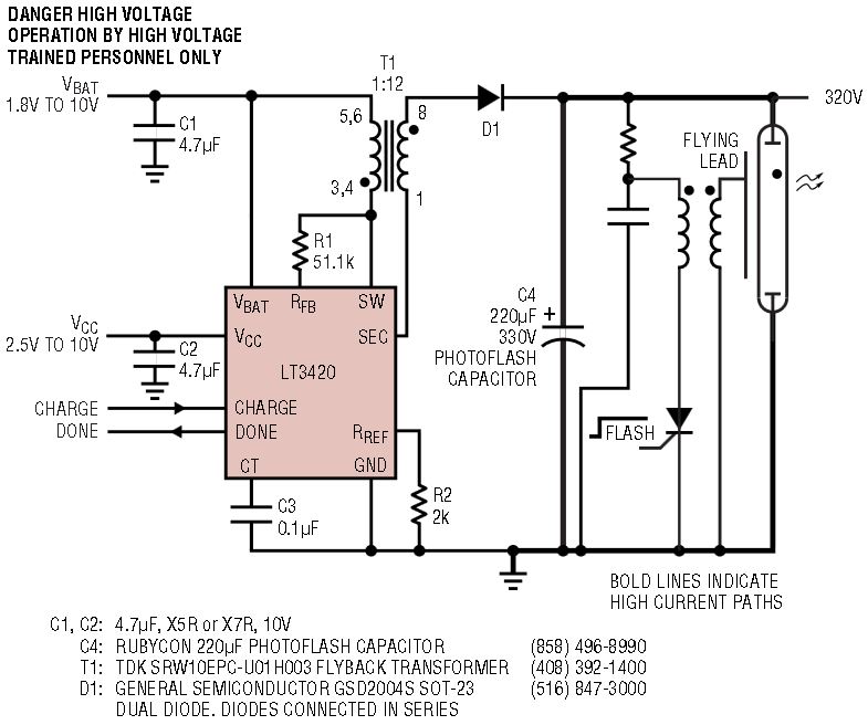
Figure 1a. 320V photoflash capacitor charging circuit.
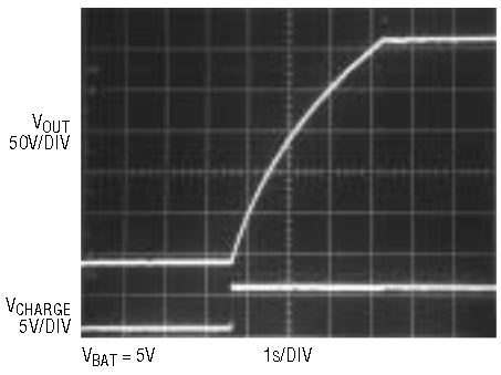
Figure 1b. Charging waveform.
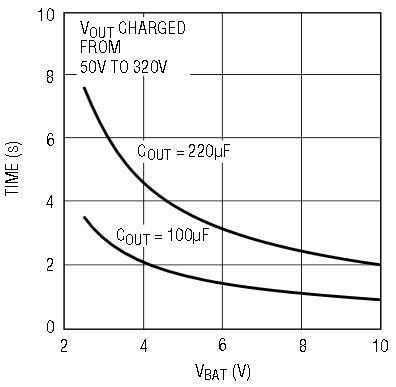
Figure 1c. Charge time.
In Figure 1a, the circuitry to the right of C4 shows a typical way to generate the light pulse once the photoflash capacitor is charged. When the SCR is fired, the flying lead placed next to the xenon bulb reaches many kilovolts in potential. This ionizes the gas inside the bulb forming a low impedance path across the bulb. The energy stored in the photoflash capacitor quickly flows through the Xenon bulb, producing a burst of light. It is important to implement the ground routing shown in Figure 1a, because during a flash, hundreds of amps can flow in the traces indicated by bold lines. Improper ground routing can result in erratic behavior of the circuit.
Figure 2 shows a simplified block diagram of the LT3420. At any given instant, the Master Latch determines which one of two modes the LT3420 is in: “Power Delivery” or “Refresh.” In Power Delivery Mode, the circuitry enclosed by the smaller dashed box is enabled, providing power to charge photoflash capacitor C4. The output voltage is monitored via the flyback pulse on the primary of the transformer. Since no output voltage divider is needed, a significant source of power loss is removed. In fact, the only DC loading on the output capacitor is due to inherent self-leakage of the capacitor and minuscule leakage from the rectifying diode. This results in the photoflash capacitor being able to retain most of its energy when the LT3420 is in shutdown.
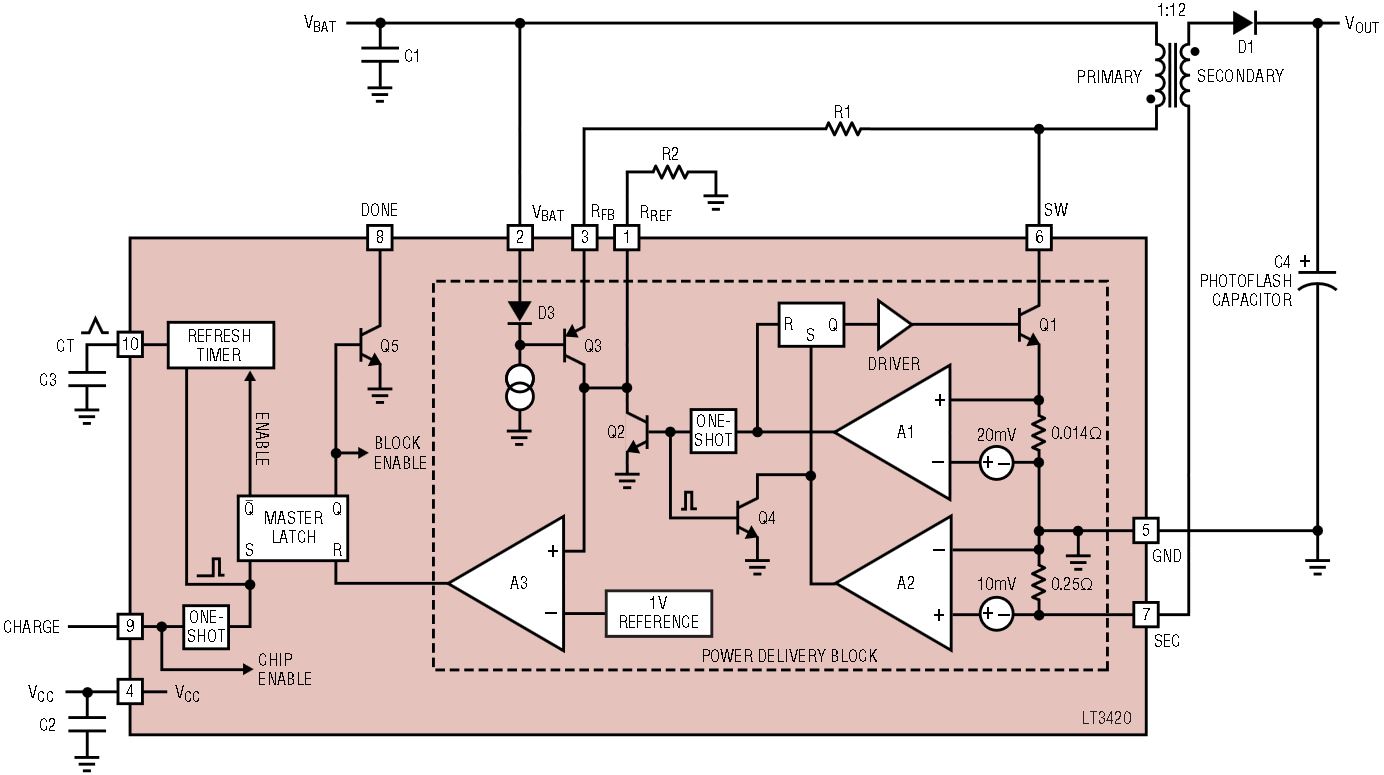
Figure 2. Simplified block diagram of the LT3420.
Once the target output voltage is reached, the power delivery mode is terminated and the part enters the refresh mode. In refresh mode, the power delivery block is disabled, reducing quiescent current, while the refresh timer is enabled. The refresh timer simply generates a user programmable delay, after which the part reenters the power delivery mode. Once in the power delivery mode, the LT3420 will again provide power to the output until the target voltage is reached. Figure 3 is an oscillogram showing both the initial charging of the photoflash capacitor and the subsequent refresh action. The upper waveform is the output voltage. The middle waveform is the voltage on the CT pin. The lower waveform shows the input current. The mode of the part is indicated below the photo.
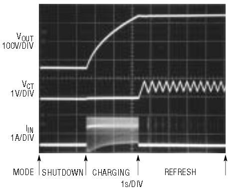
Figure 3. The three operating modes of the LT3420: shutdown, charging, and refresh of the photoflash capacitor.
The user can defeat the refresh timer and force the part into power delivery mode by toggling the CHARGE pin high then low, then high again. The low-to-high transition on the CHARGE pin fires a one-shot that sets the master latch, putting the part in power delivery mode. Bringing CHARGE low puts the part in shut-down. The refresh timer can be programmed to wait indefinitely by simply grounding the CT pin. In this configuration, the LT3420 will only reenter the power delivery mode by toggling the CHARGE pin.
In power delivery mode, the LT3420 operates by adaptively controlling the switch on-time and off-time. The switch on-time is controlled so that the peak primary current is 1.4A (Typical). The switch off-time is controlled so the minimum secondary current is 40mA (Typical). With this type of control scheme, the part always operates in the CCM (Continuous Conduction Mode), resulting in rapid charging of the output capacitor. A side benefit of this scheme is that the part can survive a short circuit on the output indefinitely. Figure 4a and 4b show the relevant currents during the power delivery mode when VOUT is 100V and 300V respectively. Notice how the on-time and off-time are automatically adjusted to keep the peak current in the primary and secondary of the transformer constant as VOUT increases.
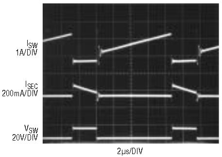
Figure 4a. Switching waveforms with VOUT = 100V, VCC = VBAT = 3.3V.
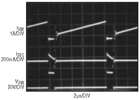
Figure 4b. Switching waveforms with VOUT = 300V, VCC = VBAT = 3.3V.
Measuring Efficiency
Measuring the efficiency of a circuit designed to charge large capacitive loads is a difficult issue, particularly with photoflash capacitors. The ideal way to measure the efficiency of a capacitor charging circuit would be to find the energy delivered to the output capacitor (0.5 • C • V2) and divide it by the total input energy. This method does not work well here because photoflash capacitors are far from ideal. Among other things, they have relatively high leakage currents, large amounts of dielectric absorption, and significant voltage coefficients. A much more accurate, and easier, method is to measure the efficiency as a function of the output voltage. In place of the photoflash capacitor, use a smaller, high quality capacitor, reducing errors associated with the non-ideal photoflash capacitor. Using an adjustable load, the output voltage can be set anywhere between ground and the maximum output voltage. The efficiency is measured as the output power (VOUT • IOUT) divided by the input power (VIN • IIN). Figure 5 shows the efficiency for the circuit in Figure 1, which was measured using this method. This method also provides a good means to compare various charging circuits since it removes the variability of the photoflash capacitor from the measurement. The total efficiency of the circuit, charging an ideal capacitor, would be the time average of the given efficiency curve, over time as VOUT changes.
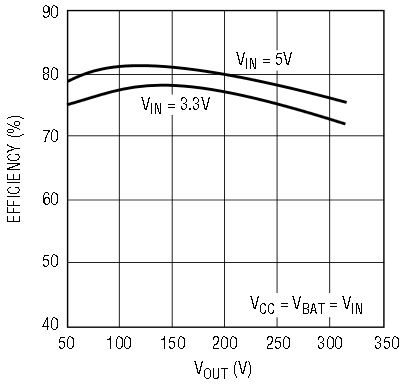
Figure 5. Efficiency for the circuit in Figure 1.
Standard Transformers
Analog Devices has worked with several transformer manufacturers (including TDK, Pulse and Sumida) to provide transformer designs optimized for the LT3420 that are suitable for most applications. Please consult with the transformer manufacturer for detailed information. If you wish to design your own transformer, the LT3420 data sheet contains a section on relevant issues.
Professional Photoflash Charger
Figure 6 shows a professional grade charger designed to charge large (>500μF) photoflash capacitors quickly and efficiently. Here, multiple LT3420 circuits can be used in parallel. The upper most circuit in the figure is the master charger. It operates as if it were the only charger in the circuit. The DONE signal from this charger is inverted by Q1 and drives the CHARGE pin of all the other slave chargers. Notice that grounding the RREF and CT pins disables the control circuitry of the Slave chargers. The charging time for a given capacitor is inversely proportional to the number of chargers used. Three chargers in parallel takes a third of the charging time as a single charger applied to the same photoflash capacitor. This circuit can charge a 650μF capacitor from 50V to 320V in 3.5s from a 5V input.
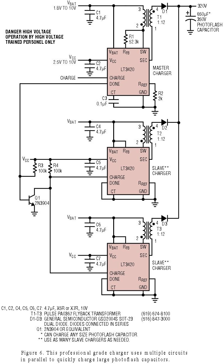
Figure 6. This professional grade charger uses multiple circuits in parallel to quickly charge large photoflash capacitors.
Interfacing to a Microcontroller
The LT3420 can be easily interfaced to a microcontroller. The CHARGE and DONE pins are the control and mode indicator pins, respectively, for the part. By utilizing these pins, the LT3420 can be selectively disabled and enabled at any time. The microcontroller can have full control of the LT3420. Figure 7 shows the LT3420 circuit being selectively disabled when the CHARGE pin is driven low midway through the charge cycle. This might be necessary during a sensitive operation in a digital camera. Once the CHARGE pin is returned to the high state, the charging continues from where it left off.
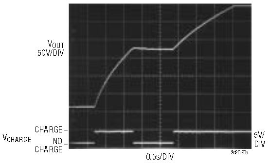
Figure 7. Halting the charge cycle at any time.
Adjustable Input Current
With many types of modern batteries, the maximum allowable current that can be drawn from the battery is limited. This is generally accomplished by active circuitry or a polyfuse. Different parts of a digital camera may require high currents during certain phases of operation and very little at other times. A photoflash charging circuit should be able to adapt to these varying currents by drawing more current when the rest of the camera is drawing less, and vice-versa. This helps to reduce the charge time of the photoflash capacitor, while avoiding the risk of drawing too much current from the battery. The input current to the LT3420 circuit can be adjusted by driving the CHARGE pin with a PWM (Pulse Width Modulation) signal. The microprocessor can adjust the duty cycle of the PWM signal to achieve the desired level of input current. Many schemes exist to achieve this function. Once the target output voltage is reached, the PWM signal should be halted to avoid over-charging the photoflash capacitor, since the signal at the CHARGE pin overrides the refresh timer.
A simple method to achieve adjustable input current is shown in Figure 8. The PWM signal has a frequency of 1kHz. When ON is logic high, the circuit is enabled and the CHARGE pin is driven by the PWM signal. When the target output voltage is reached, DONE goes high while CHARGE is also high. The output of A1 goes high, which forces CHARGE high regardless of the PWM signal. The part is now in the Refresh mode. Once the refresh period is over, the DONE pin goes low, allowing the PWM signal to drive the CHARGE pin once again. This function can be easily implemented in a microcontroller. Figure 9 shows the input current for the circuit of Figure 1 as the duty cycle of the PWM signal is varied.
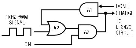
Figure 8. Simple logic for adjustable input current.
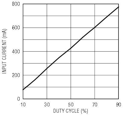
Figure 9. Input current as duty cycle is varied.
Conclusion
The LT3420 provides a highly efficient and integrated solution for charging photoflash capacitors. Many important features are incorporated into the device, including automatic refresh, tightly controlled currents and an integrated power switch, thus reducing external parts count. The LT3420 comes in a small, low profile, MSOP-10 package, making for a complete solution that takes significantly less PC board space than more traditional methods. Perhaps most importantly, the LT3420 provides a simple solution to a complicated high voltage problem, freeing camera designers to spend time on other important matters, like increasing the pixel count or adding new camera features.


