Hot Swap Controller Enforces Tracking in Split Supply Systems
Hot Swap Controller Enforces Tracking in Split Supply Systems
Dec 1 2003
Introduction
Split power supplies are widely used in audio, video and data communication systems. These systems typically use ±5V, ±12V or ±15V supply voltages and require a wide range of operating currents. The LT4220 Hot Swap controller—which operates over any combination of split supplies ranging from ±2.7V to ±16.5V—allows a circuit board to be safely inserted or removed from a live backplane without glitching the power supplies while controlling load currents from milliamps to amps.
Glitches can cause anything from objectionable “pops” in audio systems, data loss in digital systems or even connector damage. Pops can also originate from shifting bias points or complementary stages wherein half of the circuit is correctly powered and the other half has not yet been powered.
The LT4220 offers the usual Hot Swap features, such as limiting inrush current to the local supply bypass capacitors and isolating faults from the system supply should they occur, but it also coordinates voltage tracking of the split supplies. Tracking ensures that both the positive and negative supplies power-up either coincidently or ratiometrically, thereby eliminating glitch and pop problems. This complete split supply Hot Swap control system is packaged in a small 16-lead SSOP plastic package.
The LT4220
The LT4220 contains two independent, yet coupled, Hot Swap controllers, one for the negative supply and one for the positive supply. The control action is carefully coordinated such that the supplies turn on together, turn off together and in the case of an over-current fault, both outputs are tripped off simultaneously. Best of all, the LT4220 enforces active tracking between the two supplies during power-up to ease the design requirements of the split supply circuitry and eliminate abnormal circuit behavior arising from asymmetrical supply ramps.
The LT4220 provides other important Hot Swap features, including input voltage monitors, output voltage monitors, a circuit breaker with selectable automatic retry, timed current limiting with foldback, and gate drives for N-channel MOSFET devices to be used on both the negative and positive supplies.
Basic Operation
Figure 1 shows a simplified block diagram of the LT4220. The inputs are monitored and power-up is not started until both are good. The outputs are monitored and PWRGD signals when both are good. Tracking monitors the outputs via the FB pins and controls the gate drives to assure correct power-up. N-channel MOSFETs are used on both supplies, eliminating the need for complementary devices. FAULT indicates when a current limit condition has caused the timer to time out. Connecting FAULT back to ON+ enables automatic retry. Ramp rates are adjusted by gate capacitors and associated gate charging currents. Nevertheless, when track is enabled the actual rate is no faster than the slowest ramp.
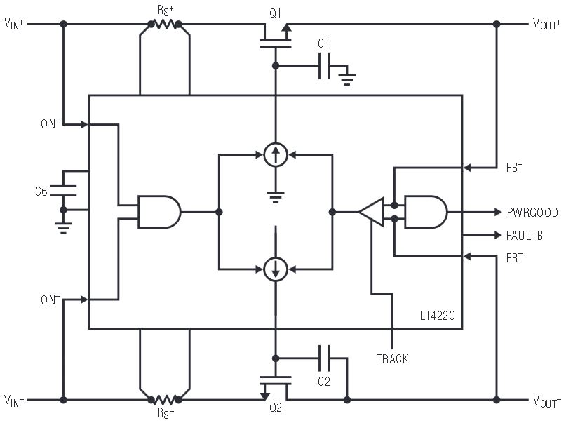
Figure 1. LT4220 Simplified block diagram.
Typical Hot Swap Application
Figure 2 shows a complete circuit design for a ±12V, 10A Hot Swap circuit using the LT4220. Q1 and Q2 N-channel MOSFET devices control the ±12V output power-up profiles after insertion. Resistors RS+ and RS– sense the load current, enabling the LT4220 to protect against temporary overloads and short circuits. R5 and R7 prevent high frequency parasitic oscillations sometimes associated with power MOSFET devices operating in their linear regions. The amount of inrush current is set by the appropriate choice of C1 and C2. In this case the inrush current is limited to approximately 100mA for a 100μF load capacitance. In case of an output short circuit, both Hot Swap channels incorporate timed current limiting with foldback to protect the MOSFET devices against over-dissipation, and disconnect a faulted circuit from the backplane. Foldback is especially valuable in difficult circumstances such as start up into a 0Ω short circuit, where simple protection schemes may not be sufficient to protect the output MOSFET devices. Resistive divider ratios for R1/R2 and R3/R4 were chosen to enable the GATE drive outputs when both input supplies are within 15% of their final value. Resistive divider ratios for R9/R10 and R11/R12 were chosen to indicate that the output power was good when both outputs are within 15% of their final value. The 15% value was chosen assuming that the system power supply tolerances were ±10%.
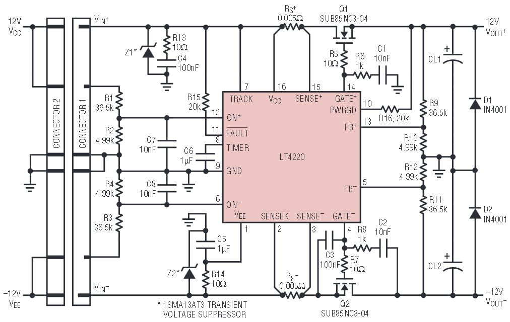
Figure 2. LT4220 ±12V, 10A Hot Swap controller.
Power-Up Sequence
Bouncing contacts and voltage glitches during board insertion wreak havoc with sensitive analog circuitry powered by split supplies. The LT4220 eliminates all of these issues (the results shown in Figure 3). After the ON+ and ON– pins exceed their undervoltage lockout thresholds, the gates of Q1 and Q2 (GATE+, GATE–) are pulled up by the internal current sources. For large capacitive loads the inrush current is limited by the gate slew rate or by the foldback current limit. For a desired inrush current that is less than the foldback current limit, the feedback capacitors C1 and C2 can be used to control the output voltage slew rates by integrating the gate pullup currents. Once both output supply voltages exceed their power good thresholds and the MOSFETs Q1/Q2 are fully enhanced, the PWRGD signal is released and pulled high by R16 (Figure 2).
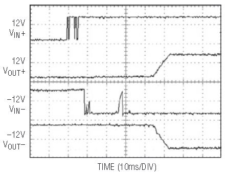
Figure 3. Power-up sequence.
Supply Tracking
When the TRACK pin is connected to VIN+, track mode is enabled. The function of this mode is to control the GATE+ and GATE– pullup currents such that the desired output voltages ramp characteristic is achieved. The gate pullup currents are controlled via the FB+ and FB– pins.
Figure 4 shows coincident tracking for a system operating with +12V and –12V supplies as per the circuit in Figure 2. The circuit in Figure 2 is easily converted to work with –5V and +12V supplies by simply changing R3, R9 and R11 to 12.4kΩ. The new coincident tracking behavior is shown in Figure 5. Ratiometric tracking is sometimes preferable, especially in signal processing applications. Figure 6 shows this mode of operation, obtained by changing only R3 and R11 to 12.4kΩ. Note that in this case the supply ramps are made to start and finish at the same time.
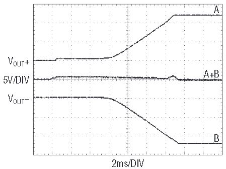
Figure 4. ±12V coincident supply tracking.
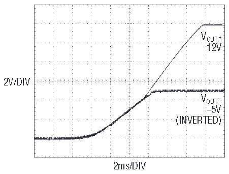
Figure 5. +12V, –5V coincident supply tracking (–5V signal inverted).
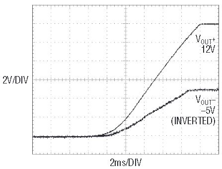
Figure 6. +12V, –5V ratiometric supply tracking (–5V signal inverted).
Short-Circuit Protection
Current limiting provides protection for the output MOSFET devices. The current limit for either supply is set by sense resistors RS+ and RS– (Figure 2). The voltage across the sense resistor is regulated by the current limit circuitry to 50mV for conditions where foldback current limiting is not enabled. The TIMER pin provides a means for setting the maximum time the LT4220 is allowed to operate in current limit. Whenever the current limit circuitry becomes active, by either the positive or negative sense amplifier operating in current limit, a pull-up current source of 60uA is connected to the TIMER pin and the voltage rises with a slope of dV/dt = 60μA/CTIMER. If the overload is removed, a small 3μA pulldown current slowly discharges the timer pin. If the timer succeeds in charging to a 1.24V threshold, an internal fault latch is set and the FAULT pin is pulled low. Both MOSFETs are quickly turned off while the TIMER pin is slowly discharged to ground.
The power dissipation will be high in the output MOSFET devices when the output is shorted with zero ohms. To prevent excessive power dissipation in these pass transistors the current limit on each supply is reduced as the output voltage falls. This characteristic, commonly referred to as “current foldback”, reduces the fault current as the output voltage drops and reaches the lowest level into the short. The foldback current limiting reduces short circuit MOSFET dissipation by a factor of 2.5. The FB± pins effectively measure the MOSFET VDS voltage and control the appropriate current limit sense amplifier input offset to provide the foldback current limit.
Automatic Restart
Normally the LT4220 latches off in the presence of a fault. Nevertheless, by removing R15 in Figure 2, you can connect the FAULT and ON+ together to enable automatic restart. FAULT pulls the ON+ pin low allowing an automatic restart to be initiated once the TIMER pin ramps below 0.5V.
Conclusion
The LT4220 combines all of the functions necessary for split supply Hot Swap control in one small 16-lead SSOP plastic package. This device is adaptable to applications covering a wide range of positive and negative supply voltages, ramping profiles, capacitance and load currents, including optical/laser, audio and ECL systems.


