Hot Swap Circuit Gets InfiniBand Power onto your Module
An InfiniBand™ backplane distributes bulk power at 12VDC to a number of plug-in modules, each having a DC/DC converter that steps the 12V supply down to the voltages required locally. A pass transistor on each module isolates the converter’s input capacitors during module plug-in, allowing modules to be added without disturbing others on the backplane. The requirements governing module hardware design are found in the InfiniBand Architecture Specification, Volume 2, Release 1.0. This article describes a circuit fully implementing the specification for sequencing bulk power. The power conversion problem is not discussed here.
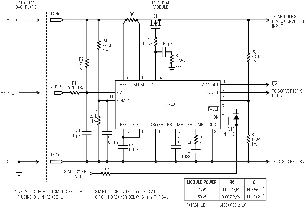
Figure 1 shows the circuit. Power is supplied from the backplane at 12VDC between VB_In and VB_Ret. There are two control signals, VbxEn_L (active low), and Local Power Enable (active high). The LTC1642 Hot Swap™ controller IC performs four functions in this circuit. It controls pass transistor Q1’s gate in response to both signals; it limits Q1’s drain current; it monitors VB_In for both overvoltage and undervoltage conditions; and starts the DC/DC converter downstream. The LTC1642 was selected because it can respond to two control inputs and because its voltage range suits the application’s requirements. Although the backplane supplies 12V nominally, the InfiniBand specification requires steady-state operation to 14VDC and up to 16V for 1ms transients; this is satisfactory because the LTC1642 is fully specified for operation up to 16.5V. Its 33V maximum rating is an added benefit: capacitive bypassing at VB_In is limited to 5nF by the specification, so high frequency ringing to voltages substantially higher than 16V after “hot” module removal or a load short is to be expected.

Figure 1. LTC1642 InfiniBand Hot Swap circuit.
During module plug-in, the circuit operates as follows. The longest pins, VB_In and VB_Ret, mate first with the backplane. The LTC1642’s OV (overvoltage) pin is pulled high by R2, holding Q1 off. OV is pulled low by R1 when the shorter VbxEn_L pin mates with the backplane, where it is shorted to VB_Ret. VbxEn_L is only asserted if the voltage at OV is less than 1.223V (±1%), so Q1 remains off if VB_In exceeds 16V DC; C1 filters out ringing. The chip also monitors VB_In for undervoltage conditions through the R3-R4 divider, holding the COMPOUT pin low when VB_In is less than 10V. COMPOUT can be tied to the ON pin to lock out undervoltages on VB_In. Local Power Enable is driven by an InfiniBand Management Device, powered separately from a 5V auxiliary, also supplied by the backplane. It is asserted at voltages greater than 1.223V (±1%). Tie it high through a 10k current limiting resistor if there is no management device on the module. After assertion of both control signals there is a delay of 20ms, which is proportional to C2, before Q1’s source begins ramping. The ramp rate, 0.5V/ms (inversely proportional to C3) safely limits the charging current drawn by the DC/DC converter’s input capacitors. R5 prevents self-oscillations in Q1, which operates as a source follower while ramping. The R7–R8 divider monitors Q1’s source voltage, with the RESET output holding the DC/DC converter off until Q1’s source voltage reaches 10V.
R6 senses Q1’s drain current. When its voltage drop reaches a limiting value, a control loop in the LTC1642 servos Q1’s gate voltage to prevent further increases in drain current. The loop regulates in 5µs to 10µs after activation, safely within the 20µs specification. R9 works with C3 to compensate this loop. Q1’s maximum allowed drain current increases as its source voltage, sensed by the R7–R8 divider, increases. The voltage across R6 is limited to 23mV when the LTC1642’s FB pin is grounded, increasing gradually to 53mV when FB is 1V or more. This “foldback” current limiting tends to equalize Q1’s power dissipation during “hard” and “soft” shorts. If Q1 remains in current limit too long, it is latched off to keep it from overheating, and the FAULT output is asserted. The delay before latch-off is 1ms, proportional to C4. R10 is included to ensure that Q1 eventually latches off after repetitive, transient current limiting individually lasting less than 1ms. Optional diode D1 is particularly useful on modules lacking an InfiniBand Management Device; it automatically restarts the LTC1642 if it should latch off. Increase C2 if using it, to increase Q1’s off time and keep it from overheating during repeated start-up cycles. To restart the circuit if D1 is omitted, either an InfiniBand Management Device must detect the fault and toggle Local Power Enable or the bulk power to the module must be cycled off then on.
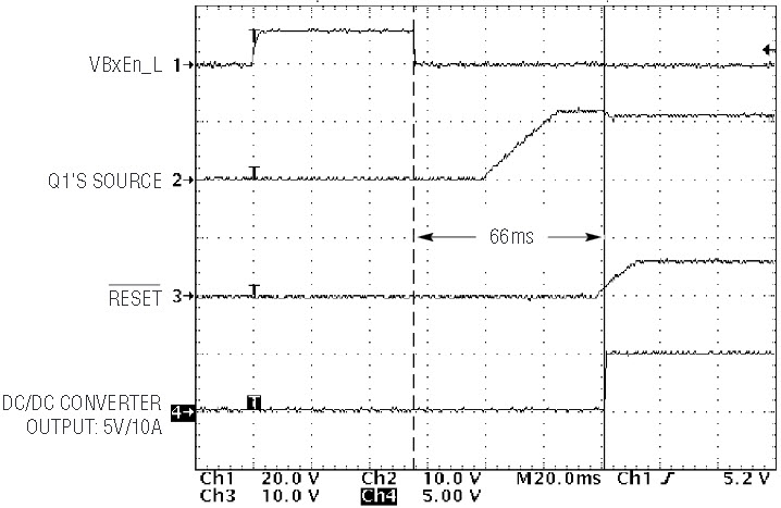
The circuit was tested with a 50W DC/DC converter, LTC Demo Board DC222 (demo boards are available to qualified customers—contact LTC Marketing for information). Figure 2 shows an oscillograph captured during module plug-in. The delay from VbxEn_L assertion to the converter’s output coming into regulation is 66ms, safely within the 500ms InfiniBand specification.

Figure 2. Waveforms during module plug-in.
InfiniBand is a trademark of the InfiniBand Manufacturers Association.


