High Power, Single Inductor, Surface Mount Buck-Boost µModule Regulators Handle 36VIN, 10A Loads
Introduction
One of the most daunting tasks for a power supply designer is producing a high power density supply where the output voltage sits within the input voltage range. High power density buck-boost converters usually require complex and bulky magnetics, run at low efficiency, and place high electrical and thermal stresses on devices. The LTM4605 and LTM4607 µModule regulators can cure these buck-boost headaches. The secret is in reducing the component selection to an inductor, a sense resistor and bulk input and output capacitors. The resulting solution is as close to a plug-and-play buck-boost converter you can get in an IC form factor.
The LTM4605 and LTM4607 incorporate most of the components needed for a complete buck-boost solution in their 15mm × 15mm × 2.8mm low profile packages, including the switching controller, power FETs and support components. Their synchronous 4-switch architecture can achieve up to 92% efficiency in boost mode and 97.7% efficiency in buck mode.
The LTM4605 has a 4.5V to 20V input range and a 0.8V to 20V output range, while the LTM4607 takes a 4.5V to 36V input to a 0.8V to 24V output. Such wide voltage ranges save significant design time as one part can serve a wide variety of applications—reducing the need to certify and stock different parts for different applications. To round out these devices as complete power supplies, both include important safety features including true soft-start, output overvoltage protection (OVP) and foldback protection in buck, boost and buck-boost modes.
12V, 5A Supply from a 5V–36V Input
Figure 1 shows the LTM4607 providing a 12V, 5A output from a 5V–36V input. The LTM4607 operates as a buck converter at input voltages above the output, as a boost converter at input voltages well below the output, and a combination of the two in the transition region where the input voltage is close to the output.
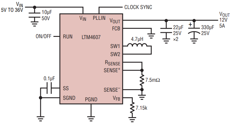
Figure 1. Remarkable simplicity in the face of an otherwise daunting task. Only a few components are required to provide an efficient 12V, 5A output from a 5V-to-36V input.
Inside the LTM4605 and LTM4607
Figure 2 is a simplified internal diagram of the LTM4607, showing the two switching legs: the boost leg connected to the output, and the buck leg to the input. Each synchronous switching leg is formed by two MOSFETs. SW1 and SW2 tap the middle of the internal boost leg and buck leg respectively.
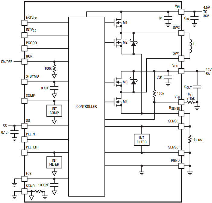
Figure 2. Simplified block diagram of the LTM4607.
Operation of the LTM4607 buck, boost and transition regions can be seen in Figures 3 to 5. In buck mode, SW1 is connected to the output and the internal buck leg switches to regulate the output voltage. In boost mode, SW2 is connected to the input and the boost leg is in action. During the transition mode, when the input voltage is close to the output, both buck leg and boost legs are in action. To keep the internal bootstrap circuits constantly alive for both legs, the “inactive” leg refreshes every tenth cycle of the “active” leg. That is, the boost leg switches once for every ten switching cycles in buck mode while the buck leg switches similarly in boost mode.
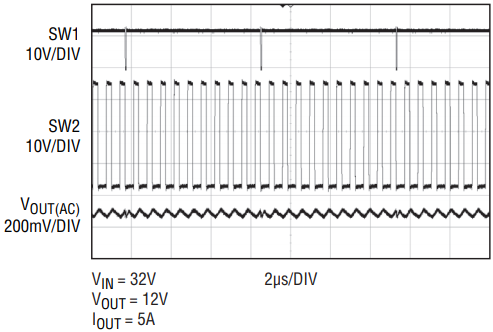
Figure 3. Buck mode waveforms.
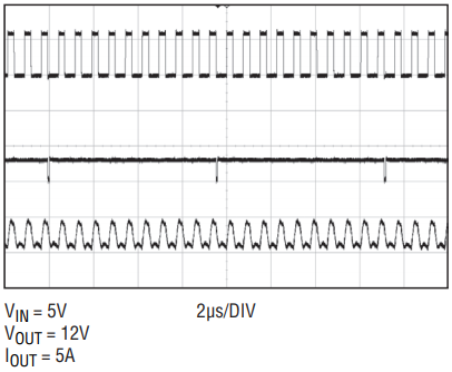
Figure 4. Boost mode waveforms.

Figure 5. Transition mode waveforms.
Efficiency Considerations
The internal MOSFETs are optimized and able to deliver up to 12A output current for the LTM4605 and 10A for the LTM4607 in buck mode. The LTM4607’s maximum output current in boost mode is rated at 5A DC (typical). Either part can be easily paralleled for higher current applications (see next section). The current limitations are imposed by power losses from the internal MOSFETs.
Figure 6 shows the typical efficiency of the LTM4607 at various input voltages. Worst-case efficiency usually occurs at minimum and maximum VIN. At minimum VIN, increased inductor current and related conduction losses take the biggest bite out of efficiency, while at maximum VIN, switching losses dominate. Derating is necessary under certain input, output and thermal conditions. Thermal images of the circuit shown in Figure 1 are shown in Figure 7. Note that Figure 7b shows a single µModule regulator supplying 10A in buck mode.
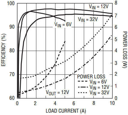
Figure 6. Efficiency and power loss for the LTM4607 at different input voltages.
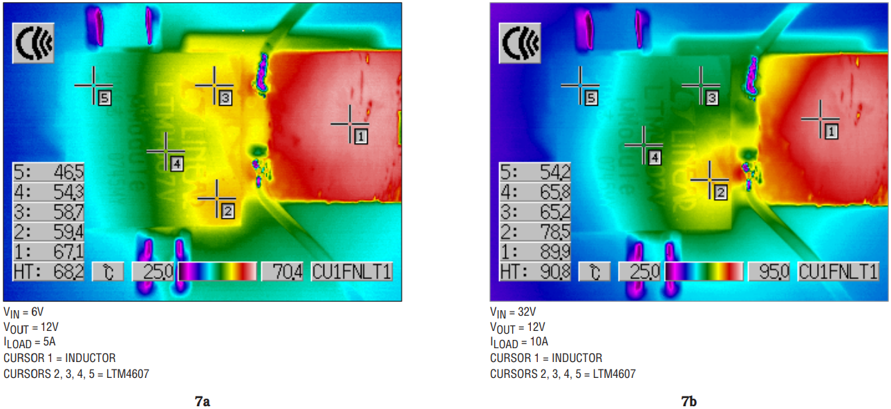
Figure 7. Thermal images with VOUT = 12V and 25°C ambient temperature.
PolyPhase® Paralleling for High Output Current
If an application requires higher current than a single LTM4605 or LTM4607 can supply, two or more µModule regulators can be connected in parallel (Figure 8) to increase the available output current. The current mode architecture of the LTM4607 facilitates efficient PolyPhase operation (interleaved switch operation) of the parallel regulators. In a parallel setup, a single VOUT set resistor is shared by the regulators. The current control signal and COMP pins are tied together, thus resulting in balanced current sharing, as shown in Figure 9.
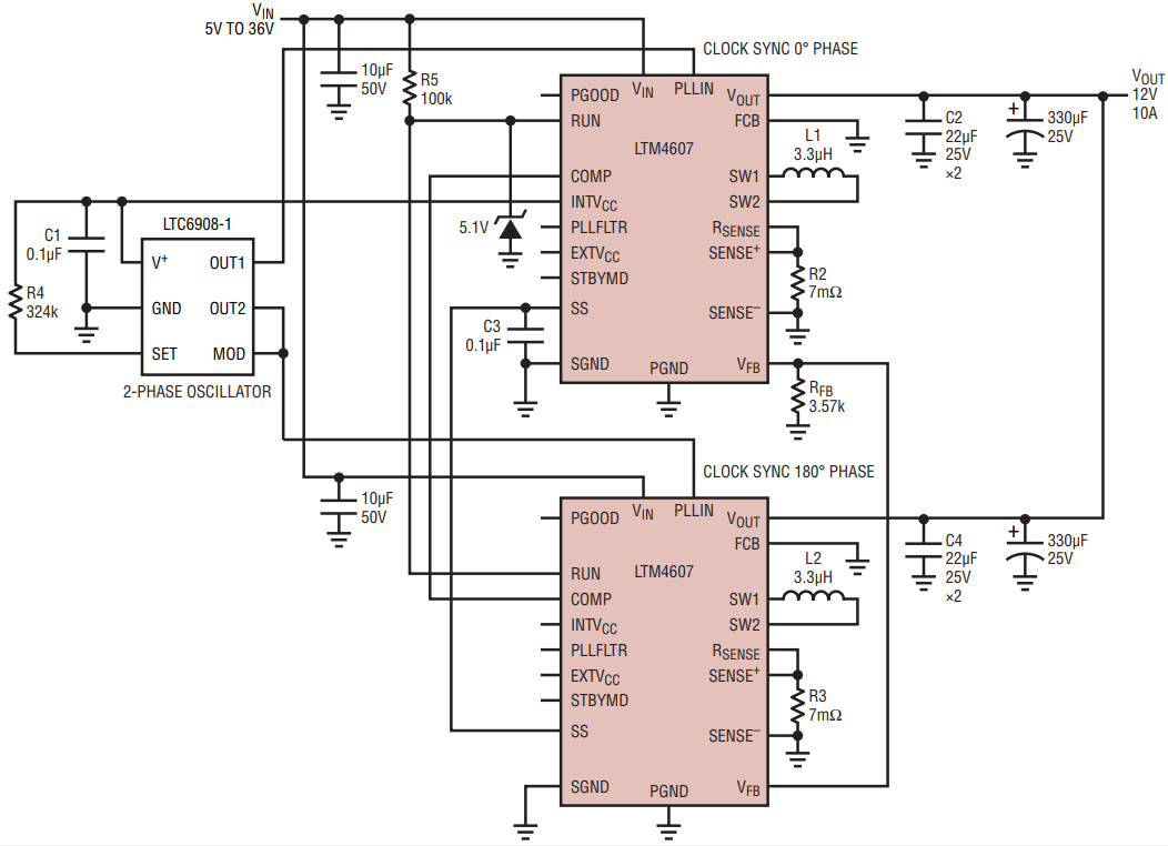
Figure 8. Schematic of two LTM4607 in parallel to provide 12V at 10A output from 6V to 36V source.

Figure 9. Inductor current waveforms at start-up and load transient with two LTM4607s in parallel.
The 200kHz to 400kHz phase lock loop of LTM4607 enables interleaved switch operation, which reduces input and output ripple current. Figure 8 shows two LTM4607s connected in parallel to provide a 12V, 10A output. Interleaved clock signals are generated by the LTC6908-1.
PCB Layout Considerations
With over 12A of inductor current and four switching MOSFETs, care must be taken during the PCB layout to minimize EMI and thermal stress. Figure 10 shows the recommended component placement of components on both the top and bottom of the board.
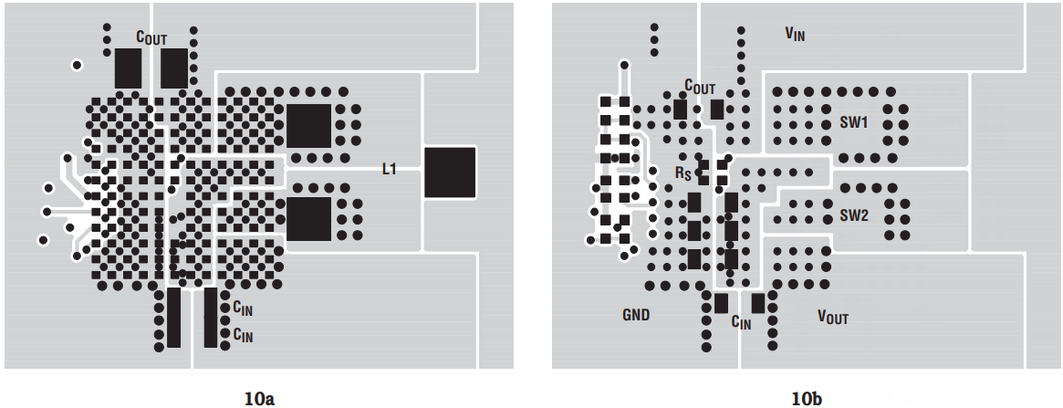
Figure 10. Recommended parts placement and layout.
There are two critical loops. One is formed by input capacitors, the SW2 pins, the sense resistor and GND; the other is formed by output capacitor, the SW1 pins, the sense resistor and GND. Because of the high dI/dt pulsing current in both loops, their area should be minimized. Thus, the sense resistor should be put directly beneath the module with as many vias as possible on RSENSE and GND. When components are restricted to one layer, place the sense resistor as close as possible to the module. Low ESR and ESL ceramic capacitors should be used at the input and output and be placed as close to the module as possible. The second layer should be a solid ground plane.
Because both the LTM4605 and LTM4607 use a versatile and responsive current mode control architecture, an external sense resistor is required. Accurate sensing of the inductor current is required for both system stability and an accurate current limit. Because the sensed current is pulsating, parasitic inductance along the current path should be minimized. A Kelvin connection is recommended as shown in Figure 11, and the current sense traces should be close to each other.1

Figure 11. Kelvin connection used to sense current.
Layout with the LTM4605 and LTM4607 couldn’t be easier—there are so few components—but it is important to carefully consider thermal design.
SW1 and SW2 nodes should be connected to a large sized copper conductor utilizing the inner and bottom layers to help dissipate heat. Thermal vias should be placed beneath the module and on the copper planes as shown in Figure 10.
Since both the SW1 and SW2 nodes produce high dV/dt values, it is better to keep control signal traces away from these nodes.
To improve reliability and thermal performance, the thermal profile should be tuned to minimize voids. Also try to place control signals in inner layers to free the thicker top and bottom layers for current conduction and thermal dissipation.
Conclusion
The LTM4605 and LTM4607 µModule regulators simplify the design of buck-boost power supplies. Their low profile 15mm × 15mm × 2.8mm packages and minimal component count help free up valuable PCB area. High input and high output ratings suit these regulators to networking, industrial, automotive systems and high power battery-operated devices. Their optimized internal 4-switch architecture provides high efficiency and high performance. Overall, the LTM4605 and LTM4607 reduce product design and test time with a mix of high performance features, flexible settings and ease-of-use.
Notes
1 For more about layout with Kelvin sense resistors, see “Using Current Sensing Resistors with Hot Swap Controllers and Current Mode Voltage Regulators” by Eric Trelewicz in Linear Technology Magazine, September 2003, page 34


