Fast CMOS Op Amp Challenges Bipolar Amps on All Key Specs
Introduction
The LTC6241 dual and LTC6242 quad CMOS op amps compete head-on with bipolar op amps in noise, speed, offset voltage, and offset drift, while maintaining superior low input bias and noise current. Crucial advances in these amplifiers’ parameters translate to tighter system specs, lower complexity, and a wider supply voltage operating range than previous CMOS op amps. These extremely low input bias current op amps are optimized for high impedance transducer applications such as photodiode transimpedance amplifiers, TIAs, though they are also well suited to a variety of precision applications.
The LTC6241 and LTC6242 do not employ complicated post-package schemes to reduce offset voltage, yet their 125µV offset voltage and 2.5µV/°C offset drift are among the best CMOS amplifiers available. The 18MHz gain bandwidth and very low noise further distinguishes them from a field of mediocre amplifiers. They are fully specified on 3V, and 5V, with an HV version that guarantees operation to ±5.5V. Supply current consumption is 2.2mA/amplifier maximum. Table 1 summarizes the conservative specs for these op amps.
| Parameter | Conditions | Min | Typ | Max | Units | |
| Offset Voltage | VCM = 0 S8, LTC6241 GN16, LTC6242 DD, DHC, LTC6241/42 |
40 50 100 |
125 150 550 |
µV µV µV |
||
| TC VOS | ● | 0.6 | 2.5 | µV/°C | ||
| Input Bias Current | ● |
1 10 |
75 |
pA pA |
||
| Noise Voltage | f = 1kHz f = 0.1Hz to 10Hz |
7 550 |
10 | nV/√Hz nVP–P |
||
| Noise Current | f = 100kHz | 110 | fA/√Hz | |||
| Input Capacitance | f = 100kHz CDM CCM |
0.5 3 |
pF pF |
|||
| Large Signal Gain | RL = 1kΩ to VS/2 | 90 | 215 | V/mV | ||
| CMRR | VCM = –V to +V – 1.5V | ● | 80 | 105 | dB | |
| Operating Supply Range | LTC6241/42 LTV6241HV/42HV |
● ● |
2.8 2.8 | 6 11 |
V V |
|
| VOUT Low | ISINK = 5mA | ● | 190 | 325 | mV | |
| VOUT High | ISOURCE = 5mA | ● | 4.81 | 4.675 | V | |
| Supply Current | per amplifier | ● | 1.8 | 2.2 | mA | |
| Slew Rate | AV = –2, RL = 1kΩ, | ● | 5 | 10 | V/µs | |
| Gain Bandwidth Product | RL = 1kΩ | ● | 13 | 18 |
The LTC6241 is available in the SO8, and for compact designs it is packaged in the tiny dual fine pitch leadless (DFN) package. The LTC6242 is available in a 16-Pin SSOP as well as a 5mm × 3mm DFN package.
CMOS with Low 1/f Noise? What about Noise Current?
CMOS op amps have traditionally had much higher 1/f noise than bipolar amplifiers. It is common to find CMOS amplifiers with a 1/f corner above several kilohertz, but the LTC6241 rivals the best bipolar op amps with a 1/f noise corner of only 40Hz. This exceptionally low noise translates to just 550nVP–P in a 0.1Hz to 10Hz bandwidth, and represents the lowest 1/f noise available in a non-autozero CMOS op amp.
In I-to-V applications such as photodiode amplifiers, where the amplifier is operated inverting, noise current dominates at high frequency. CMOS op amp noise current has two sources. The first is the input device channel thermal noise coupling through the gate-to-source and gate-to-drain capacitances. The second noise current is derived from the op amp’s input capacitance, and capacitance associated with the input transducer. This input referred noise current (CV noise) is due to the amplifier’s noise voltage, VN, impressed across the total input capacitance, CT, causing a current of magnitude 2πfCTVN to flow through the feedback resistor.
The way to make CMOS or bipolar low noise amplifiers is with large input transistors. The problem is that big input structures carry the burden of high input capacitance. High input capacitance increases high frequency noise current, as well as reduces overall op amp speed. An uncommon feature of the LTC6241 is its low differential input capacitance of just 0.5pF, which is a major benefit in I-to-V amplifier designs. This input capacitance is 8 to 10 times lower than than that of other CMOS amps.
Simple Architecture Yields Low Noise and DC Precision
Figure 1 is a simplified schematic of one half of the LTC6241, which has a pair of low noise input transistors M1 and M2. A simple folded cascode Q1, Q2, and R1, R2 allow the input stage to swing to the negative rail, while performing level shift to the differential drive generator. Transistors M1 and M2 along with current sources I1 and I2 have been optimized for low noise and consume over 30% of the die area. Low offset is achieved by laser trimming resistors RT1 and RT2. Stresses that occur during package assembly have minimal affect on this simple, stable architecture, and consequently, complicated post-package trim schemes that adjust offset voltage and drift are unnecessary.
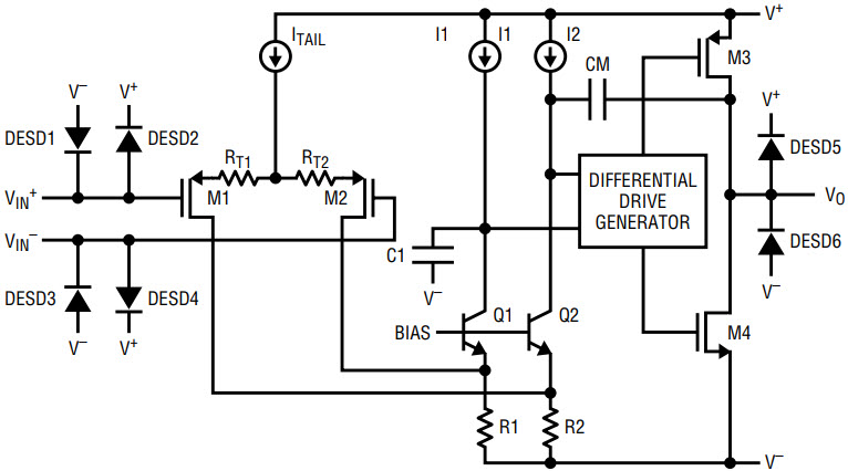
Figure 1. Simplified schematic
The LTC6241 and LTC6242 were intentionally designed without a rail-to-rail input stage as to not compromise their noise specs. Many CMOS rail-to-rail input amplifiers show large offset shift and higher noise when the common mode voltage is operating in this top side transition region, limiting their usefulness.
The LTC6241 and LTC6242 have reverse-biased ESD protection diodes on all inputs and outputs as shown in Figure 1. These diodes protect the amplifiers from ESD strikes up to 1.7kV. No current flows into the gate on a DC basis, but these ESD protection diodes are the source of input bias current specified on the data sheet. These diodes have leakage current that doubles approximately every 7°C, but input current typically remains below 10pA up to 85°C ambient.
Capacitor C1 reduces the unity cross frequency and improves the frequency stability without degrading the gain bandwidth of the amplifier. Capacitor CM sets the overall amplifier gain bandwidth. The differential drive generator supplies signal to transistors M3 and M4 that swing the output from rail-to-rail.
Figure 2 shows the distribution of offset voltage and offset voltage drift. Figure 3 shows the input bias current vs common mode voltage as well as the noise voltage and current spectrum.
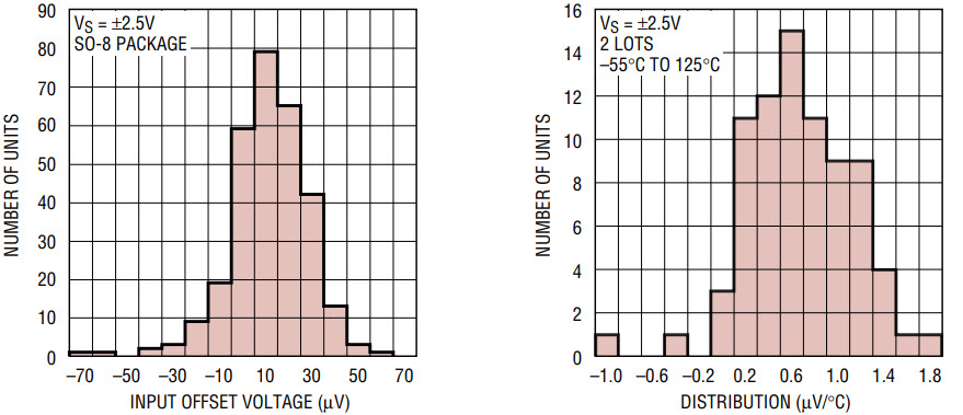
Figure 2. VOS distribution and VOS temperature coefficient distribution

Figure 3. Input bias current vs common mode voltage and voltage and current noise vs frequency
Applications
Non-Inverting Integrator
Integrators are used widely in feedback control systems and filters. CMOS input amplifiers like the LTC6241 are preferred for this function because the low input bias current allows the use of large value resistors and small capacitors for a given integration time constant. The most common form of integrator is the inverting form, shown in Figure 4. It has a transfer function of:

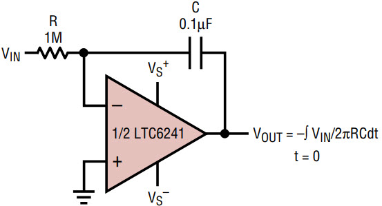
Figure 4. A textbook integrator is inverting
If inversion is not desired in the feedback control loop using the circuit in Figure 4, a designer must add another op amp to invert again. A simpler overall solution produces a non-inverting integrator using just one op amp. Figure 5 shows the circuit.
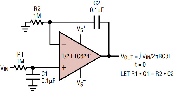
Figure 5. A non-inverting integrator can be very simple. Ideally, R1 • C1 = R2 • C2, but mismatch is inevitable. To avoid any phase buildup from a mismatch, the time constants may be skewed so that R1 • C1 < R2 • C2.
At low frequencies, R1 • C1 does not attenuate, and the non-inverting integration function is provided by the op amp gain and its feedback components C2 and R2. At higher frequencies, C2 becomes a short circuit so the op amp goes to a gain of one, and the integration function is provided by R1 and C1. If the time constants are matched, the integrator conformance is excellent. Matching is not easy. In most loops, to guarantee that the phase of the integrator does not exceed 90 degrees, the time constants can be intentionally skewed so that R1 • C1 < R2 • C2. For an example of a specific closed loop utilization of a non-inverting integrator, see LTC Design Note DN254.
Piezoelectric Accelerometers:
Inverting vs Non-Inverting
Figures 6 and 7 show two different approaches to amplifying signals from a capacitive sensor using the LTC6241. The sensor in both cases is a 770pF piezoelectric shock sensor accelerometer, which generates charge under physical acceleration. Figure 6 shows the classical “charge amplifier” approach. The op amp is in the inverting configuration so the sensor looks into a virtual ground. All of the charge generated by the sensor is transferred across the feedback capacitor by the op amp action. Because the feedback capacitor is 100 times smaller than the sensor, the output is forced to a voltage 100 times what would have been the sensor’s open circuit voltage. Thus, the circuit gain is 100.
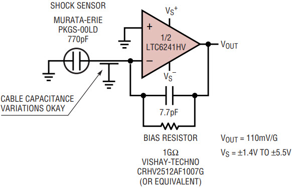
Figure 6. Classical inverting charge amplifier. Variations in cable capacitance (i.e. length) do not affect the signal gain. Use this circuit when the accelerometer is remote from the amplifier and the cable length is unspecified. Drawbacks are that gain is set by the low valued feedback capacitor and low frequency performance is set by the bias resistor working into the same.
The benefit of this approach is that the signal gain of the circuit is independent of any cable capacitance introduced between the sensor and the amplifier, making this a good solution for remote accelerometers where the cable length may vary. Difficulties with the circuit are inaccuracy of the gain setting with the small capacitor, and low frequency cutoff due to the bias resistor working into the small feedback capacitor.
Figure 7 shows a non-inverting amplifier approach. This approach has many advantages. First, the gain is set accurately with resistors rather than with a small capacitor. Second, the low frequency cutoff is dictated by the bias resistor working into the large 770pF sensor, rather than into a small feedback capacitor, for lower frequency response. Third, the non-inverting topology can be paralleled and summed (as shown) for scalable reductions in voltage noise. The only drawback to this circuit is that the parasitic capacitance at the input reduces the gain slightly. This circuit is favored in cases where parasitic input capacitances such as traces and cables are relatively small and invariant.
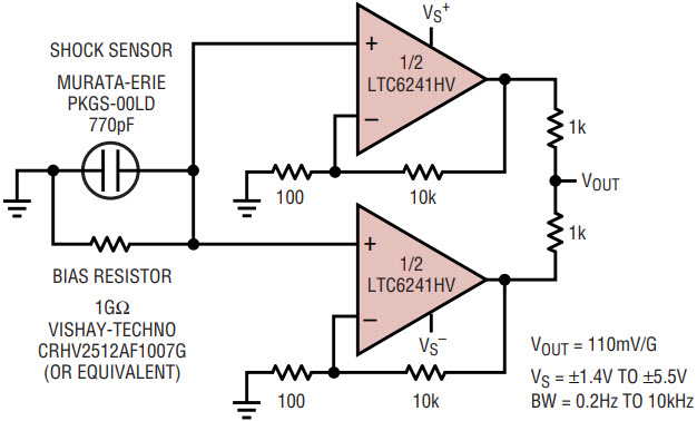
Figure 7. Non-inverting charge amplifier offers several advantages. Stages can be paralleled for lower voltage noise. Bias resistor works into higher capacitance for better low frequency response.
Consider making the bias resistor larger than bandwidth calculations would suggest. This actually reduces the noise floor at low frequency. For example, to support frequencies down to 10Hz at –3dB, the bias resistor would calculate to:

At 10Hz, the 20M r esistor would contribute 580nV/√Hz of noise, and be 3dB down just like the signal. Making the resistor 1GΩ as shown, its 4000nV/√Hz voltage noise would be attenuated down to effectively 80nV/√Hz by the accelerometer capacitance, while the signal would barely be attenuated at all. That’s an easy seven-fold improvement in the signal-to-noise ratio.
Large Area Photodiode Amplifiers
Figure 8 shows the LTC6241 used as a transimpedance amplifier for a high capacitance large area photodiode. The circuit has unity noise gain at DC, so resolution is entirely noise limited. The bandwidth rolls due to the fact that the photodiode impedance drops with frequency raising the effective gain (the noise gain), which the op amp looks into. This severely limits the bandwidth and increases the output noise. The –3dB bandwidth for this circuit was measured at 25kHz, and the output noise density at 10kHz was measured at 1.6µV/√Hz. That may be good enough for many applications. If it’s not good enough, keep reading.
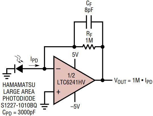
Figure 8. Large area photodiode amplifier provides about 25kHz bandwidth. DCs are good but output is noisy.
The main problem with the previous circuit is the large capacitance of the photodiode. The perfect thing to do is to bootstrap that capacitance with a low noise JFET. Figure 9 shows the circuit. The low noise JFET source follower runs about 1mA down through the 4.99k resistor, with the source sitting about 0.6V above ground. Now the effective input voltage noise placed across the photodiode capacitance is the 1nV/√Hz of the JFET rather than the 8nV/√Hz of the op amp. The op amp is looking into its own 3pF of input capacitance plus the 2pF of gate-drain capacitance, plus parasitics. That’s a much better situation than looking into 3000pF!
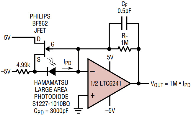
Figure 9. A simple bootstrap circuit drastically improves the ACs while leaving the DCs excellent. Output noise is now 221nV/√Hz at 10kHz, and bandwidth is 220kHz. Rise time is 1.58µs from a 3000pF photodiode at 1MΩ of gain!
The effects of this simple modification are drastic. The compensation capacitor CF can be reduced, and bandwidth is improved to 220kHz (1.58µs rise time). Output noise density at 10kHz is reduced to 221nV/√Hz, as shown in Figure 10. DC performance remains excellent because the JFET is not involved; it simply provides a slight reverse bias to the photodiode
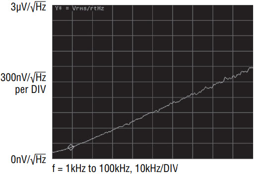
Figure 10. Output noise spectral density of the bootstrap circuit of Figure 9
Conclusion
The LTC6241 and LTC6242 combine the low noise, offset, and drift of the best bipolar op amps with low input bias and noise current of CMOS op amps. These amplifiers operate from 2.7V to ±5.5V and represent all-in-one solutions for fast, low noise signal processing.
