Dual 60µA 10-Bit Serial DAC in MS-8 Saves Power and Space
Introduction
The LTC1661 is a dual, serially addressable 10-bit, rail-to-rail voltage output DAC with Sleep mode. Operating on a single 2.7V–5.5V supply rail, its small size and low power consumption make it most appropriate for use in products with stringent space and/or power constraints. In the 8-lead MSOP package, it occupies just 0.02in2 of board space, 50% less area than a standard SO-8 package; each buffered DAC draws just 60µA of supply current at 5V (48µA at 3V). Sleep mode operation further reduces total supply-plus-reference current to just 1µA.
The LTC1661 has a reference-to-output gain of one and the REF pin can be tied to VCC for ratiometric, 0V-to-VCC output without the use of a separate reference. Each of the output amplifiers is stable driving capacitive loads of up to 1000pF, so the designer need not be concerned with the capacitance of long board traces. The serial interface is SPI/MICROWIRE™-compatible and uses a simple, flexible control word that allows the addressing of individual DACs; the data path is double buffered to allow for simultaneous updates. The digital inputs have internal Schmitt triggers, which eliminate the need for external Schmitts when the input signals are slow or noisy, such as when using optoisolators. The block diagram of the LTC1661 is shown in Figure 1.

Figure 1. LTC1661 block diagram: each DAC draws just 60µA at 5V. Double-buffered input logic allows simultaneous updates.
Performance
Load Driving
Despite its tiny operating current, the LTC1661 can deliver substantial load currents; Figure 2 shows output voltage vs load current performance. At VCC = 5V, the LTC1661 can drive over 20mA into a grounded load, the equivalent of driving a 250Ω load over the full 0V-to-VCC range. The output impedance is just 0.5Ω.

Figure 2. The LTC1661 drives over 20mA into a grounded load at 5V.
The LTC1661 output amplifiers have been optimized for driving capacitive loads (see Figure 3). Capacitances of up to 1000pF, or greater than or equal to 10µF, may be driven directly; in between these values, a small resistor may be inserted in series with the load to successfully drive any capacitance. The example in Figure 3 shows a 20Ω resistor placed in series with a 1µF load to stabilize the combination.

Figure 3. Allowable capacitive loads; the rail-to-rail output amplifiers have been optimized for driving capacitance.
Linearity
The LTC1661 uses a patented architecture that guarantees monotonicity over the full industrial temperature range. Differential nonlinearity (DNL) is typically ±0.1LSB (±0.75 max) (see Figures 4 and 5).
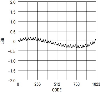
Figure 4. LTC1661 integral nonlinearity (INL).

Figure 5. LTC1661 differential nonlinearity; patented architecture guarantees monotonicity.
Operation
Serial Interface
The simple-yet-flexible SPI/MICROWIRE-compatible interface uses a 16-bit input word, which is divided into Control and Data sections (see Figure 6). The Control section of the word specifies the desired operation and selects one or both DACs to receive the instruction, whereas the Data section specifies the DAC input code. Data is captured on the rising edge of the clock with CS/LD held at a logic low. Once the full 16-bit word has been captured, the rising edge of CS/LD executes the instruction.

Figure 6. The simple 3-wire interface is used for software control of the individual DAC channels. Loading of input codes, updates and Sleep mode control are all available.
Conclusion
Low supply current, power-saving Sleep mode and extremely compact size make the LTC1661 ideal for battery-powered devices, while its ease of use, high performance and wide supply range make it an excellent choice for a wide spectrum of voltage adjustment and trimmer potentiometer applications.
MICROWIRE is a trademark of National Semiconductor Corp.


