Digital Power Sequencing
Power Sequencing is a key component of Digital Power Architectures. In this post we will take a look at several ways to architect sequencing, and its consequences. In particular, we will see how design choices impact flexibility late in the design process.
Building Blocks of Power Conversion
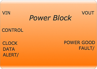
Let’s take a look at our power building blocks and tools and see what kinds of trouble we can make for ourselves. To keep things simple, let’s assume we have one universal power block (UPB), and all the usual culprits like FPGAs and Micro Controllers, and Logic. Our UPB has a simple interface:

Figure 1. Power Block
Our simple power converter has single VIN/VOUT, a PMBus interface, one input signal: CONTROL, and two output signals: POWER GOOD and FAULT/.
Control
The CONTROL signal turns the output on and off. It is active high, has an internal pull-up.
Power Good
The POWER GOOD signal is high when the output is powered, and it is in the valid range.
Fault/
The FAULT/ signal is active low, open drain, and asserted when the power block has a fault. If there is a fault, ALERT/ is asserted, and the fault can be read via the PMBus. Not all power converters will have both a POWER GOOD, and a FAULT/, and we don’t need both. FAULT/ can be the stunt double for POWER GOOD in almost every case.
Design One
Now let’s build something so we can tear it down and build another, getting better each time.
Let’s suppose we have a system with an Intermediate Bus Controller (IBC) and the following rails:
- 48V
- 19V
- 5.0V
- 3.3V
- 1.2V
- 0.8V
We decide to structure the rails as a hierarchy. But, we need a different control structure for power up.

Figure 2. Simple Power Structure
Don’t worry about whether the power hierarchy is correct or the logic is correct for any real design. What matters is the impact of this “type” of structure. Let’s consider the pros and cons of this.
On the pro side, this is simple, both conceptually and for implementation. It would be very easy to add LED indicators or read the power good with the GPIO of an FPGA or uP. If something faulted, the POWER GOOD would let the system know a rail went down.
On the con side, if there is a failure, and if the system must shutdown all the supplies, there have no choice but to shut them down in the same order that they power up. This means that the rails most down stream are going to power down by loss of power, rather than by their control pin.
There is no timing control, so extra circuits would have to be added to put delays between rails. If you added a delay between rails, the delay will only apply to power on, because at power off, loss of power on a feeder rail will take down its dependent rail before POWER GOOD can take it down.
If you make any mistakes with this “type” of structure, the PCB will require a re-layout, and while you are waiting for that, you will have no choice but to hack wires on your design, or go have a very long coffee break.
Design Two
We can do better if we centralize the logic. A programmable device, such as an FPGA or uP can manage all the logic.

Power Structure With Controller
With all the logic lines routing to GPIO, the Controller has complete control over the sequencing order, both on and off, and complete control over timing. It can be changed anytime one is willing to change Verilog or C code. I have indicated the PMBus on the controller, but not drawn all the connections, but with the PMBus, the Controller now can also control levels, and fault behavior.
On the pro side, this design is flexible, and you are not trapped. If you make a mistake in the control structure, you can fix it without a re-layout.
On the con side, you have to change Verilog or C, and possibly re-test and re-qualify the firmware. This design also requires a lot of routing. Each POL requires 5 control lines, and they are routed to the Controller individually. Suppose we had a 20 rail system, accounting for PMBus, it would require 42 GPIO pins.
So this design is flexible, but requires a lot of GPIO and a lot of PCB real estate.
Design Three
We can simplify the Controller by using the nature of the Open Drain controls, when combined with PMBus, and intelligent Digital Power POLs.

Simplified Controller
All the CONTROL pins are wired together, and all the FAULT/ pins are wired together. This means a 20 rail system only needs 5 connections. This is an 8X reduction in the number of IO pins.
Let’s see how this can work. The CONTROL pin is active high. It is controlled by GPIO0, which is set to Open Drain. Because the CONTROL pin is Open Drain, this means the POL can also pull it low.
When the POL resets, it will pull the CONTROL pin low until it is ready to respond to an external signal. This means that if the Controller is too fast, none of the POLs will turn on until they are all properly reset, and the slowest POL reset determines when the system powers up. If the Controller is slower, it controls power up when it releases the CONTROL line.
You may wonder about sequencing. Have we lost control over that? No, because PMBus has a TON_DELAY command and its value is normally stored in NVM of the POL. It can either be set by the controller, or stored in NVM using an external tool.
The FAULT/ pins are also open drain and controlled by GPIO1, and they are both input and output. This means that when any rail faults, all rails are notified when the FAULT pin is pulled low. Also, when the FAULT/ is pulled low, ALERT/ asserted. Therefore, the Controller knows there is a fault. Everybody knows, that is the key to this design.
Now you can choose a couple of options with respect to fault handling. The PMBus can respond to the ALERT/ with an Alert Response Address (ARA), which gets the address of all POLs with a fault, and then queries each POL for the fault information. It can then use a decision tree and shut down rails as needed, and in any order. Or it can shut down all rails at once and let the PMBus TOFF_DELAY manage the timing.
Many POLs have enhanced fault management and can respond to the fault directly (remember, FAULT/ is also an input). Typical responses are:
- Retry
- Immediate Off
- Ramp Off
When the POL has these advanced features, it takes a lot of burden off the Verilog or C code because the POLs can be programmed with an external tool (By PMBus and an external interface and Software). Furthermore, the response to faults is much faster than the response of processing ALERT/ when using the FAULT/ pin.
Trade-offs of Design Three
If you have enhanced POLs, there are trade-offs one can make. If fault logic is too complex for a shared FAULT/ line, simply add a Controller. If the fault logic is simple, you can configure fault behavior with a tool and you don’t need a controller. Or, you can use a Controller for telemetry and other functions, but use the FAULT/ pins for fault handling, and if you find it can’t handle all cases, you can always add code for fault handling and change it.
There are similar trade-offs with the CONTROL pin. You can use PMBus in place of that as well. In that case, the CONTROL pins still hold off turn on until all POLs have completed reset.
The maximum flexibility occurs when the CONTROL pin and FAULT pin are shared, and there is a Controller for the PMBus. With this design, there is total flexibility after the PCB is fabricated.
Power Good
In case you did not notice, I did not use the POWER GOOD. You don’t need to know when one rail is good before turning on another. If a rails are all controlled by TON_DELAY, and a is not ready in time, there will be a fault. PMBus defines TON_MAX_FAULT_LIMIT, which defines how long a rail has to ramp up and get within tolerance. If a rail is not within specification by this time, a fault occurs, which will prevent other rails from turning on.
The design principle is: no news is good news. If the system needs to know when all rails are up, all you need is a simple timer set to the longest time defined by all the TON_DELAYs. Or, the controller can make PMBus queries of the status of the last POL, etc.
In some devices, the FAULT/ pin can be reconfigured as a POWER GOOD pin. This allows you to have POWER GOOD if you really need it, but the fault sharing pin is lost. So you may want a Controller to respond to ALERT/. Or in a simpler system, ALERT/ could grab the CONTROL pin and shut down all the rails if there is a fault.
In practice, POWER GOOD is generally not necessary. But if you really want one, you can typically reconfigure the FAULT/. After all, there are always special cases. Perhaps there is always room for that “Universal Adapter Kit.”
Let’s Review
So here it is in a nut shell for those skipped ahead to the end:
The first design used what I call “Event Sequencing”. The POWER GOOD pin was connected to the CONTROL of the next POL. However, there was no configurability, and no control of fault behavior. The second design used a Controller and all ordering was put in its command, but it uses a lot of GPIO, and you are forced to have the Controller do everything.
The third design used open drain pins to share the CONTROL and FAULT/, and there was an optional Controller. This design had a lot of flexibility, a small number of GPIO pins, and simple routing. This is the most popular design approach, when the main trade-off being the decision about the controller. Much more will be said about this trade-off in future posts.
There is nothing wrong with Design One and Design Two, if you understand and can live within their constraints. But we all know the rules of the game can suddenly change during system qualification when some unexpected problem crops up. Even if you don’t think you need Design Three it is a great insurance policy. All I can say is that if I was the Power Engineer and had a big team of engineers depending on my design, I would not want to be boxed into a corner when something goes wrong. Something tells me they won’t be too happy if I delay a product release.


