DC Accurate Driver for the LTC2377-20 Achieves 2ppm Linearity
DC Accurate Driver for the LTC2377-20 Achieves 2ppm Linearity
by
Guy Hoover
Jan 10 2014
Introduction
As resolution and sample rates continue to rise for analog-to-digital converters (ADCs), the driver circuitry for the ADC analog input, not the ADC itself, has increasingly become the limiting factor in determining overall circuit accuracy. First, the driver circuitry must buffer the input signal and provide gain. In addition, it must level shift or convert a single-ended signal to a fully differential signal to satisfy the input voltage range and common mode requirements of the ADC. All must be done without adding distortion to the original signal.
This design note presents a simple ADC driver circuit that converts a ±10V single-ended input signal into a fully differential signal capable of driving the LTC2377-20 20-bit SAR ADC with a combined linearity error of only 2ppm. Options for providing higher input impedance and a lower overall supply current are also examined.
Circuit Description
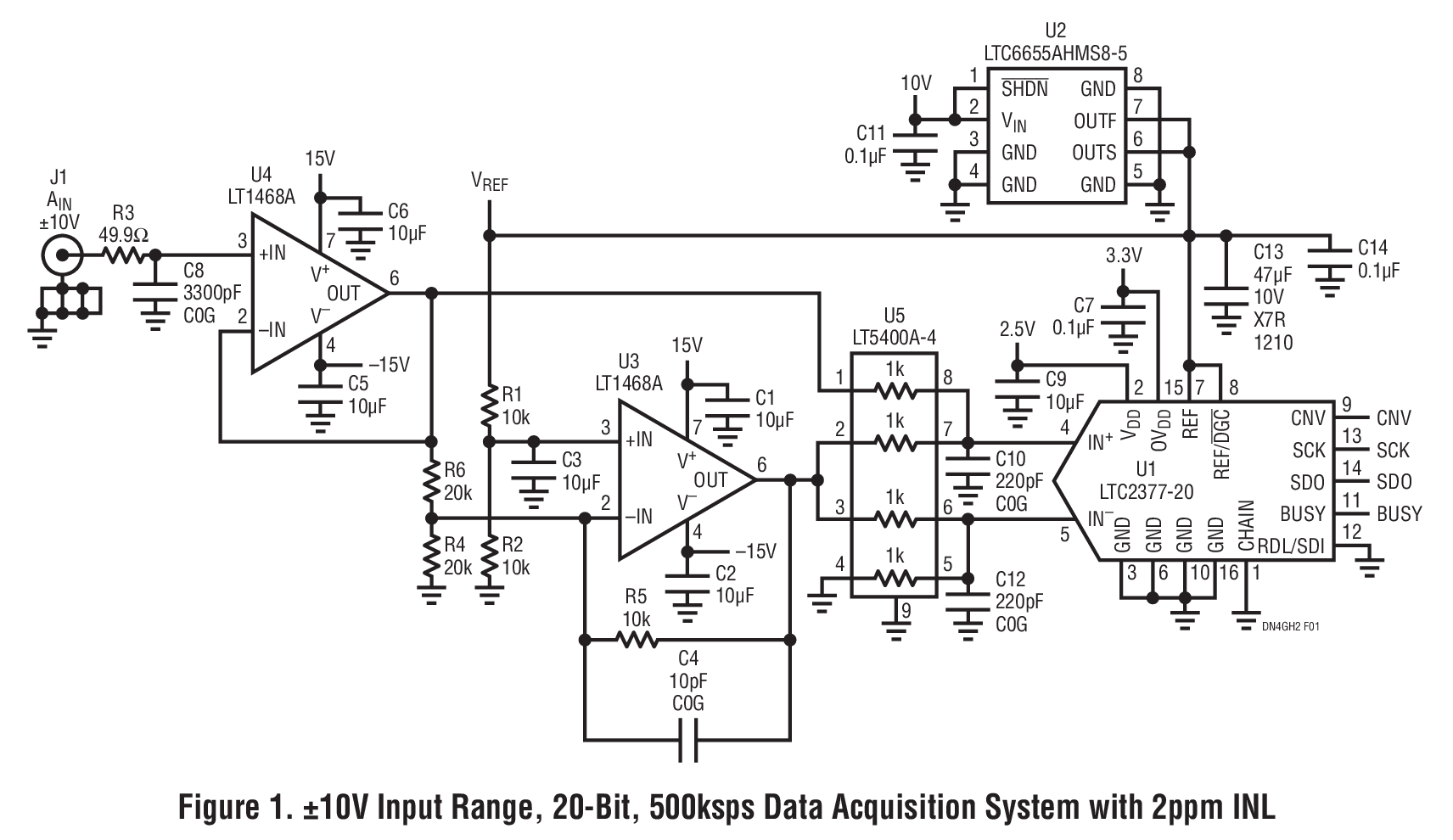
The circuit of Figure 1 converts a ±10V single-ended signal into the ±5V fully differential signal required by the LTC2377-20 (U1). The LTC2377-20 is a 20-bit, 500ksps, low power SAR ADC with a typical integral nonlinearity (INL) of ±0.5ppm. The voltage at AIN is buffered by U4, which in turn drives the U5 resistor string, acting as a precision divider. U3 operates in a gain of minus one-half and drives the center of the U5 resistor string to maintain the ADC common mode voltage at VREF/2.

U3 and U4 are LT1468A low offset highly linear op amps. U5 is a LT5400A quad matched resistor network with a guaranteed maximum mismatch of 0.01%. Matched resistor values in U5 are important because any mismatch contributes to both offset and full-scale error in this circuit. For this reason and because of their extremely low voltage coefficient, do not use discrete resistors instead of the LT5400A. R4 provides a quarter-scale shift to the output of U3. R1and R2 form a divider that biases the noninverting input of U3 at VREF/2.
R5 and R6 set the gain of inverting amplifier U3 at –0.5. C10 and C12 in combination with the resistors of U5 form 1.4MHz filters on the ADC inputs. Additionally, the resistor between Pins 1 and 8 of U5 helps to isolate the output of U4 from the charge spike that occurs when the ADC goes from hold mode to sample mode. The LTC6655A-5 (U2) was selected as the reference for this circuit due to its ability to settle quickly from the transients that occur on the REF pin during conversions and because of its low noise.VREF/2.
Circuit Performance
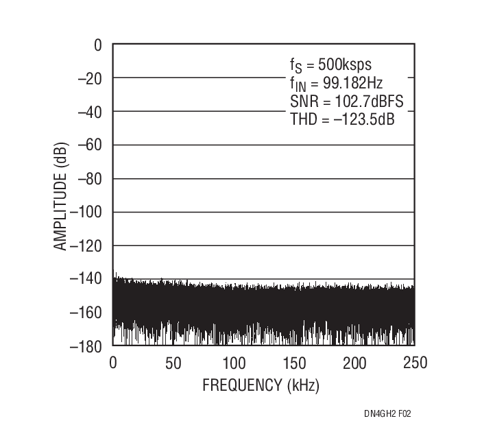
Typical AC performance for this circuit includes THD of –123.5dB and SNR of 102.7dBFS at a sample rate of 500ksps with a 100Hz input signal. This performance can be seen in the FFT of Figure 2. The THD and SNR performance are close to the typical numbers found in the LTC2377-20 data sheet, indicating minimal performance degradation when using this driver.

Figure 2. Combined Circuit FFT
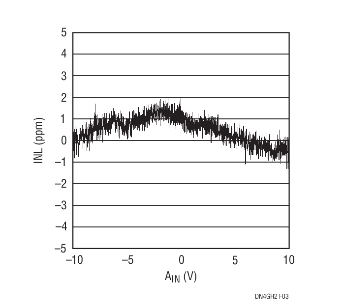
Typical linearity performance for the combined circuit over the entire ±10V input signal range, as shown in Figure 3, is +2ppm, –1.3ppm at a sample rate of 500ksps. Linearity is limited by the INL of the ADC and the CMRR of op amp U4.

Figure 3. Linearity vs Input Voltage
The combined offset at the ADC input, including the contributions of U4, U5 and U1, was measured at +50μV. The offset of U3 has no effect on the offset of this driver. A worst case analysis of offset at the ADC input is calculated by adding the maximum offsets of U1, U4 and U5:
VOS(MAX) = BZE(Max)U1 + VOS(MAX)U4/2 + (VREF/2 – VREF/(2 + ΔR/R(Max)U5))
VOS(MAX) = 13ppm • 10μV/ppm + 75μV/2 + (5/2 – 5/(2.0001)) • 1E6μV
VOS(MAX) = 292μV = 29.2ppm
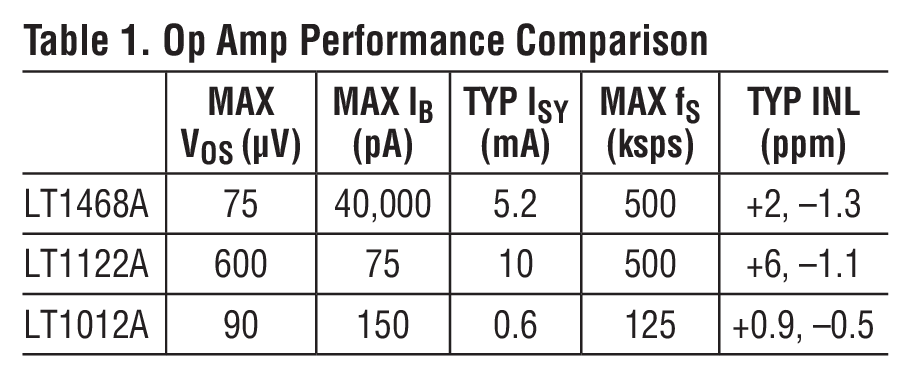
The LT1468A has a maximum input bias current of ±40nA. For applications that require higher input impedance, U4 can be replaced with the LT1122A. The LT1122A is a fast settling, JFET input op amp with a maximum input bias current of 75pA. Using the LT1122A in this circuit, the INL is +6ppm, –1.1ppm, as shown in the op amp performance comparison in Table 1.

Table 1. Op Amp Performance Comparison
The LTC2377-20 ADC has a typical supply current of 4.2mA at its full sample rate of 500ksps. The LTC2377‑20 automatically powers down after a conversion and does not power up until the next conversion is started. This auto power-down feature reduces the power dissipation of the ADC as the sample rate is reduced to as little as 1μA for very low sample rate applications.
For low sample rate applications where supply current is important, the 5.2mA maximum supply current of the LT1468A may be too high. The LT1012A picoamp input current, microvolt offset, low noise op amp with a maximum supply current of 500μA at ±15V can replace the LT1468A for these applications. With sample rates up to 125ksps the LT1012A achieved a linearity of +0.9ppm, –0.5ppm, as shown in the op amp performance comparison in Table 1. At sample rates above 125ksps the INL performance begins to degrade, as the op amp cannot settle fast enough to accurately drive the ADC.
Conclusion
The ADC driver circuit shown here converts a single-ended ±10V signal into a ±5V fully differential signal for the LTC2377-20 500ksps SAR ADC. Combined circuit performance achieves 50μV offset, 2ppm INL, 102.7dBFS SNR and –123.5dB THD. The driver consists primarily of two LT1468A op amps and a LT5400A matched resistor array. Alternative versions of this circuit use the LT1122A op amp to provide 75pA max input current or the LT1012A op amp at reduced sampling rates to reduce supply current. DC2135, a demo board version of this circuit, is available from Analog Devices.
About the Authors
Guy Hoover is an engineer with over 30 years of experience at Linear Technology as a technician, an IC design engineer and an applications engineer.
He began his career at LTC as a technician, learning from Bo...
He began his career at LTC as a technician, learning from Bo...


