Compact, Versatile, Accurate, 3-State Programmable Power Supply Supervisors
Compact, Versatile, Accurate, 3-State Programmable Power Supply Supervisors
Feb 1 2004
Introduction
Many modern electronic systems must know when the power supply (or supplies) is present and stable before start up. A power supply monitor fills this need by generating a Power-Good signal when all is ready. Likewise, once running, most systems require that the supply monitor indicate when the power supply has dropped to a minimum threshold—to prevent unreliable operation and possibly initialize housekeeping operations. An accurate supply monitor helps to avoid spurious resets and increases up-time (see "Why is Threshold Accuracy Important?" in this article).
Four new power supply supervisors improve system reliability by offering very accurate reset thresholds. They save design time, production costs and board space with simple interfaces and extremely low part count.
The LTC2904, LTC2905, LTC2906 and LTC2907 dual supervisors can simultaneously monitor two supply voltages with 1.5% threshold accuracy over temperature. The LTC2904 and LTC2905 offer nine user-selectable 2-voltage combinations from the following: 5.0V, 3.3V, 2.5V, 1.8V, 1.5V, 1.2V and 1.0V. The LTC2906 and LTC2907 offer one adjustable input and another user-selectable input, which can be either 5.0V, 3.3V or 2.5V. All four parts can be programmed to have either a 5%, 7.5% or 10% power supply tolerance.
Simple 3-state input pins (three in the LTC2904 and LTC2905, two in the LTC2906 and LTC2907) perform the threshold and tolerance programming. The part programmability removes the need to qualify, source and stock different parts for different combinations of supply voltages, providing tremendous versatility. These new parts require no software, no calibration and no trimming. Furthermore, the simple 3-state programming interface eliminates any need for external components, therefore saving additional costs and board space.
Other available features include a user-adjustable reset time-out period via an external capacitor (LTC2905 and LTC2907), or an internal capacitor for a fixed 200ms reset time-out period (LTC2904 and LTC2906). All four devices also include early availability of the reset signal so that it can be used as a reliable POR signal during power-up. In order to ensure this early availability, power must be applied to the monitor circuitry early in the power-up phase. In the LTC2904 and LTC2905 power is derived automatically from the greater of the voltages on the V1 and V2 inputs. Similarly in the LTC2906 and LTC2907, power is derived automatically from the greater of the voltages on the V1 and VCC inputs. With V1, V2 or VCC at 1V or greater, the RST output logic low is 0.3V (max) while sinking 100μA.
Therefore, the LTC2904, LTC2905, LTC2906 and LTC2907 supervisors offer micropower operation, small size and high accuracy. The highly integrated functionality makes these devices easy to design into systems requiring two or more supervisory applications. Table 1 shows a feature summary of these four devices and Figure 1 shows a typical dual supply monitor application using the LTC2904.
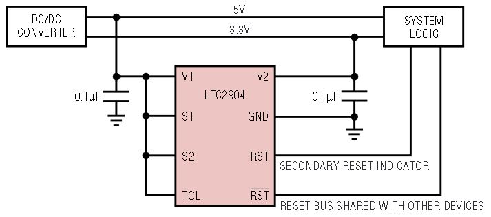
Figure 1. Fixed 5V, 3.3V supply monitor with 5% tolerance.
| Feature | LTC2904 | LTC2905 | LTC2906 | LTC2907 |
| Programmable Input Threshold Combinations | 9 | 3 | ||
| Low Voltage Adjustable Input (0.5V) | — |
— |  |
 |
| Monitored Supply Tolerance | User Selectable between 5%, 7.5% and 10% | |||
| Open Drain RST |  |
|||
| Open Drain RST |  |
— |  |
— |
| Reset Time-Out Period | Fixed 200ms | Adjustable | Fixed 200ms | Adjustable |
| Optional Supply Pin to High Availability Supply | — | — |  |
 |
| Package | 8-Lead Plastic SOT-23 or 8-Lead Plastic DFN (3mm × 2mm) | |||
Why is Threshold Accuracy Important?
Supervisor reset threshold accuracy affects the reliability of power-supply-sensitive systems. Diminished accuracy reduces reliability and corresponds to a system that must operate reliably over a wider voltage range, which complicates system design. Improved accuracy decreases the voltage range required for reliable system operation, simplifying the design.
Consider a 5V system with a ±10% power supply tolerance band (see Threshold band diagram below). System ICs powered by this supply must operate reliably within this band (and a little more, as explained below).
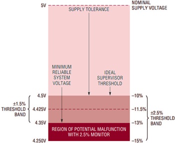
Threshold band diagram. Improved under-voltage monitor threshold accuracy translates to improved system reliability.
The bottom of the supply tolerance band, at 4.5V (5V minus 10%), is the exact voltage at which a perfectly accurate supervisor would generate a reset. Such an ideal supervisor does not exist—the actual reset threshold varies over a specified band (±1.5% for the LTC2904, LTC2905, LTC2906 and LTC2907 ). Figure 2 shows the typical threshold accuracy of the four new devices over temperature.
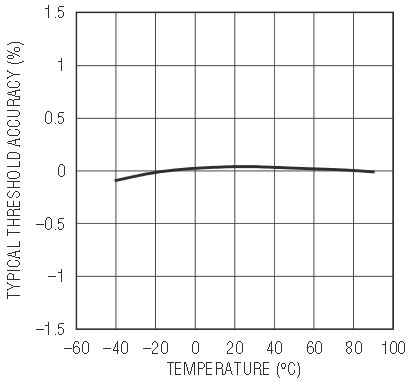
Figure 2. Typical threshold accuracy over temperature.
To prevent spurious resets, the nominal reset threshold of the supervisor is set below the minimum supply voltage, just enough that the reset threshold band and the power supply tolerance bands do not overlap. If the two bands overlap, the supervisor could generate a false or nuisance reset when the power supply is within its specified tolerance band (say, at 4.6V).
To prevent band overlap using a monitor with ±1.5% reset threshold accuracy, the 10% reset thresholds are actually set to 11.5% below the nominal input voltage. For the 5V input, the typical threshold is 4.425V, or 75mV below the ideal threshold of 4.5V. The actual threshold is guaranteed to lie in the band between 4.35V and 4.5V over temperature.
The system must work reliably down to the low end of the threshold band or risk malfunction before a reset signal is properly issued. In our 5V example, the system ICs must work down to 4.35V with a 1.5% accurate supervisor. The same system using a ±2.5% accurate supervisor must operate down to 4.25V, which is 15% lower than the nominal supply voltage, increasing the required system voltage margin and the probability of system malfunction.
Noise Sensitivity
In any supervisory application, supply noise riding on the monitored DC voltage can cause spurious resets, particularly when the monitored voltage is near the reset threshold. A less desirable but common solution to this problem is to introduce hysteresis around the nominal threshold, but hysteresis introduces an error term in the threshold accuracy. Therefore, a ±2.5% accurate monitor with ±1.0% hysteresis is equivalent to a ±3.5% monitor with no hysteresis.
The four new supervisors discussed here take a different approach to solve this problem. The first line of defense against this spurious reset for these supervisors is a first order low pass filter at the output of each of the comparators. Thus, the comparator output is integrated over time before triggering the output logic. Any transient at the input of the comparator must be of sufficient magnitude and duration before it triggers a change in the output logic. Figure 3 shows the typical transient duration versus comparator overdrive required to trip the comparators (overdrive shown as a percentage of the trip threshold VRTX).
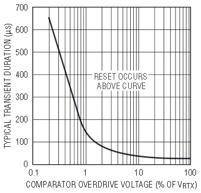
Figure 3. Typical transient duration vs comparator overdrive.
The second line of defense is the reset time-out period tRST (200ms for the LTC2904 and LTC2906 and adjustable for the LTC2905 and LTC2907 using an external capacitor). This time-out period eliminates the effect of any supply noise at a frequency above 1/tRST on the RST and RST outputs.
When either V1 or V2 drops below its programmed threshold, the RST pin asserts low (RST weakly pulls high). Then when the supply recovers above the programmed threshold, the reset-pulse-generator timer starts counting while RST stays low. If the supply remains above the programmed threshold when the timer finishes counting, the RST pin weakly pulls high (RST asserts low). However, if the supply falls below the programmed threshold at any time while the timer is still counting, the timer resets. The timer begins counting again when the supply next rises above the programmed threshold.
Note that this second line of defense is only effective for a rising supply and does not affect the sensitivity of the system to a falling supply. Therefore, the first line of defense that works for both rising and falling supplies is necessary. These two approaches prevent spurious resets caused by supply noise without sacrificing the threshold accuracy.
Although the comparators in all four supply monitors have built-in glitch filtering, bypass capacitors on V1 and V2/VCC are recommended since the greater of V1 or V2/VCC is also the internal VCC for the chip (a 0.1μF ceramic capacitor is satisfactory in most applications). A decoupling capacitor on the VADJ pin of the LTC2906 and the LTC2907 is allowed and recommended in extremely noisy environments.
3-State Programming Pins
The three 3-state input pins (S1, S2 and TOL) in the LTC2904 and LTC2905, and the two 3-state input pins (S1 and TOL) in LTC2906 and LTC2907 should be connected to GND, V1 or left unconnected during normal operation. Note that when left unconnected, the maximum leakage current allowable from the pin to either GND or V1 is 10μA.
In margining applications, all of the 3-state input pins can be driven using a TRI-STATE buffer. The low and high output of the TRI-STATE buffer must satisfy the VIL (0.4V) and VIH (1.4V) of the 3-state input pins. Moreover, when the driving TRI-STATE buffer is in the high impedance state, the maximum leakage current allowed from the pin to either GND or V1 is 10μA. Figure 4 shows the LTC2904 used in a margining application with all 3-state pins driven by a TRI-STATE buffer (Fairchild 74LVX125).
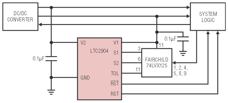
Figure 4. LTC2904 in margining application.
Monitor Programming
Connecting S1 and S2 to GND, V1 or leaving them open selects the LTC2904 and LTC2905 input voltage combinations. Table 2 shows the nine possible combinations of nominal input voltages for the LTC2904 and LTC2905, and their corresponding S1, S2 connections.
| V1 | V2 | S1 | S2 |
| 5.0 | 3.3 | V1 | V1 |
| 3.3 | 2.5 | Open* | GND |
| 3.3 | 1.8 | V1 | Open* |
| 3.3 | 1.5 | Open* | V1 |
| 3.3 | 1.2 | Open* | Open* |
| 2.5 | 1.8 | GND | GND |
| 2.5 | 1.5 | GND | Open* |
| 2.5 | 1.2 | GND | V1 |
| 2.5 | 1.0 | V1 | GND |
| *Open = open circuit or driven by a TRI-STATE® buffer in high impedance state with leakage current less than 10μA. | |||
Similarly, for the LTC2906 and LTC2907, connecting S1 to GND, V1 or leaving them open selects the V1 input voltage threshold. Table 3 shows the three possible combinations of the V1 nominal input voltage for the LTC2906 and LTC2907, and their corresponding S1 connection.
| V1 | S1 |
| 5.0 | V1 |
| 3.3 | Open |
| 2.5 | GND |
Tolerance Programming
Tolerance of either 5%, 7.5% or 10% for the supply is set at the TOL pin. The tolerance applies to both the V1 and V2 input voltages for the LTC2904 and LTC2905, or the V1 and VADJ input voltages for the LTC2906 and LTC2907. A larger tolerance lowers the trip threshold. Table 4 shows the tolerances selection corresponding to a particular connection at the TOL pin.
| Tolerance | TOL |
| 5% | V1 |
| 7.5% | Open |
| 10% | GND |
The Adjustable Input (LTC2906, LTC2907)
The non-inverting input on the VADJ comparator is set to 0.5V (Figure 5) when the TOL pin is set high (5% tolerance). The high impedance inverting input directly ties to the VADJ pin. In typical applications, this pin connects to a tap point on an external resistive divider between the positive voltage being monitored and ground. The following formula obtains the trip voltage at 5% tolerance from the resistors value:

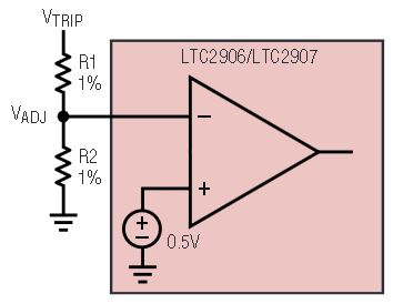
Figure 5. Setting the adjustable trip threshold.
Once the resistor divider is set in the 5% tolerance mode, there is no need to change the divider for the other tolerance modes (7.5%, 10%) because the internal reference is scaled accordingly. Table 5 shows suggested 1% resistor values for various adjustable applications.
| VSUPPLY (V) | VTRIP (V) | R1 (k) | R2 (k) |
| 12 | 11.25 | 2150 | 100 |
| 10 | 9.4 | 1780 | 100 |
| 8 | 7.5 | 1400 | 100 |
| 7.5 | 7 | 1300 | 100 |
| 6 | 5.6 | 1020 | 100 |
| 5 | 4.725 | 845 | 100 |
| 3.3 | 3.055 | 511 | 100 |
| 3 | 2.82 | 464 | 100 |
| 2.5 | 2.325 | 365 | 100 |
| 1.8 | 1.685 | 237 | 100 |
| 1.5 | 1.410 | 182 | 100 |
| 1.2 | 1.120 | 124 | 100 |
| 1.0 | 0.933 | 86.6 | 100 |
| 0.9 | 0.840 | 68.1 | 100 |
| 0.8 | 0.750 | 49.9 | 100 |
| 0.7 | 0.655 | 30.9 | 100 |
| 0.6 | 0.561 | 12.1 | 100 |
User Adjustable Reset Time-Out Period
The reset time-out period (tRST) for LTC2905 and LTC2907 is adjustable in order to accommodate a variety of applications. Connecting a capacitor, CTMR, between the TMR pin and ground sets tRST. The following formula determines the value of capacitor needed for a particular reset time-out period:

For example, using a standard capacitor value of 22nF would give a 22000/110 = 200ms delay.
Figure 6 shows the desired delay time as a function of the value of the timer capacitor that should be used. Leaving the TMR pin open sets the reset time-out to approximately 200μs. The only limitation to the length of the period is the value of the capacitor and its leakage. The TMR capacitor does not charge if the leakage current exceeds the TMR charging current of 2μA (typical).
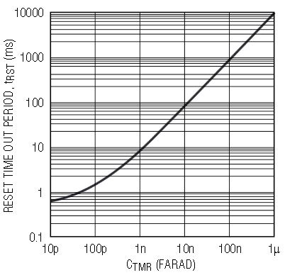
Figure 6. Reset time out period (tRST) vs capacitance (CTMR).
Circuit Description
Internally all four new supervisors include two extremely accurate comparators, a bandgap reference, accurate resistor ladders, TRI-STATE detector, CMOS decoding logic, counters, and an oscillator. Figure 7 shows the generic functional block diagram representation for all four devices. Note that only some of the pins shown in the diagram are available in any one supervisor (see Table 1).
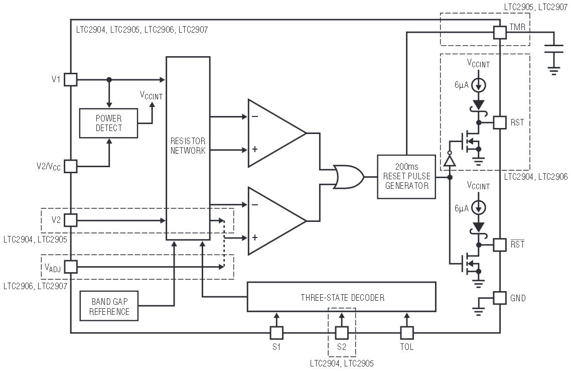
Figure 7. Block diagram representation of LTC2904, LTC2905, LTC2906 and LTC2907.
Note that both RST and RST have weak internal pull-ups to internal VCC and a strong pull-down to ground. The weak pull-up and strong pull-down arrangement allows these two pins to have open-drain behavior while possessing several other beneficial characteristics. The weak pull-ups eliminate the need for external pull up resistors when the rise time on these pins is not critical. On the other hand, the open-drain RST configuration allows for wired-OR connections and can be useful when more than one signal needs to pull down on the RST line.
Applications
3.3V, 1.2V Dual Supply Monitor at 7.5% Tolerance with LED Power Good Indicator
Figure 8 shows the LTC2904 configured as a dual monitor in an application for a system using a 3.3V and 1.2V supply. In this particular application the monitor is configured to have 7.5% tolerance. With a guaranteed 2.5mA pull-down current at the RST pin, an LED can be used in series with a 499Ω pull-up resistor as a power good indicator.
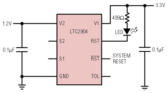
Figure 8. 3.3V, 1.2V monitor at 7.5% tolerance with LED power good indicator.
3.3V, 2.5V, 0.8V, 0.6V Quad Supply Monitor with 5% Tolerance
Figure 9 shows an LTC2906 and an LTC2907 cascaded together to monitor four voltages. In this particular application, the two supervisors are configured to monitor 3.3V, 2.5V, 0.8V and 0.6V, each with 5% tolerance. The RST outputs of the two supervisors are wired-OR together to form a master system reset. Because of the open-drain configuration on the RST pin, the master system reset is low once any of the four voltages goes below their respective thresholds. The additional RST pin on the LTC2906 can be used as a secondary reset indicator, indicating which of the two supervisors issues the reset in a particular reset condition.
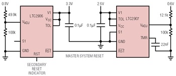
Figure 9. Quad supply monitor for 3.3V, 2.5V, 0.8V, 0.6V with 5% tolerance.
A 22nF capacitor sets the reset time-out period of the LTC2907 to 200ms for the 2.5V and 0.6V inputs. The LTC2906 reset time-out period is preprogrammed by an internal capacitor to 200ms for the 3.3V and 0.8V inputs.
The VCC pins on both LTC2906 and LTC2907 can be connected to any highly available secondary supply of at least 2.5V. Connecting the VCC pin to a high-availability supply ensures that the supervisors’ output is valid for inputs at V1 and VADJ down to 0V. However, connecting the VCC pin to the V1 pin as shown in Figure 9 only guarantees a valid supervisor output for V1 input down to 1V.
5V, 3.3V Dual Supply Monitor with Voltage Margining Application for Automated On-board Testing
In high reliability system manufacturing and test, it is desirable to verify the correct operation of electrical components at or below the rated power supply tolerance. The supervisors introduced here complement such testing in two ways.
First, a test-module can provide more supply headroom by lowering the reset trip thresholds for automated onboard testing. Using the 3-state programming input pin TOL, the global supply tolerance can be set to 5%, 7.5% or 10%. Figure 10 shows an LTC2905 used in such an application.
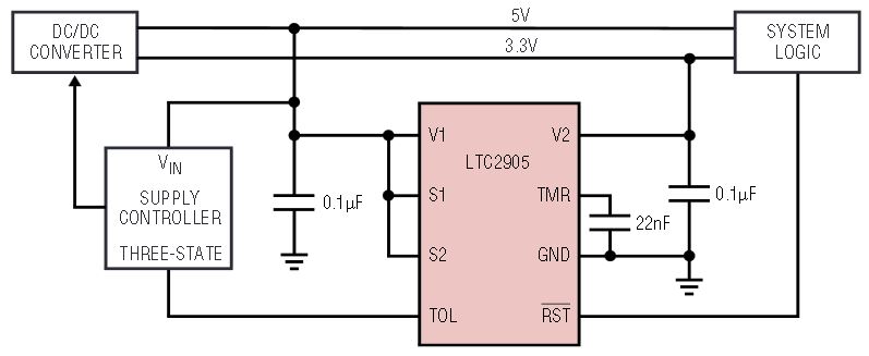
Figure 10. 5V, 3.3V dual supply monitor with voltage margining application for automated onboard testing.
Second, the S1 and S2 pins can be driven by 3-state outputs for a more aggressive lowering of the trip threshold. For example, in Figure 10 the S1 and S2 pins are tied to V1 to configure the part to monitor 5V and 3.3V. If TRI-STATE buffers are added to drive the S1 and S2 pins, these pins can be set to GND during testing. Connecting S1 and S2 to GND configures the LTC2905 to monitor 2.5V and 1.8V, a significant change in trip threshold from the 5V and 3.3V thresholds respectively. During normal operation, the TRI-STATE buffers can set S1 and S2 back to V1 (High) so that the part is again configured to monitor 5V and 3.3V.
Conclusion
The LTC2904, LTC2905, LTC2906 and LTC2907 micropower dual supervisors provide the space saving, simplicity, versatility, accuracy and reliability required in a wide variety multi-voltage monitoring applications. Input supply combinations are programmable without external components. The LTC2906 and LTC2907 also include a low voltage positive adjustable threshold. The comparators are 1.5% accurate over temperature and feature built-in noise rejection. Reset state is correct for internal VCC down to 1V. Reset time-out periods in the LTC2905 and LTC2907 are user adjustable with external capacitors. Power supply margining features include real-time supply tolerance and voltage threshold selections.
TRI-STATE is a registered trademark of National Semiconductor Corp.
About the Authors
Eko Lisuwandi has been a design engineer at the Analog Devices Boston Design Center since 2002. Eko spent his early career developing supervisory and high voltage power path mixed signal products in CMOS technology. Late...
Related to this Article
Products
PRODUCTION
Precision Dual Supply Monitors with One Pin-Selectable Threshold and One Adjustable Input
PRODUCTION
Precision Dual Supply Monitors with One Pin-Selectable Threshold and One Adjustable Input
PRODUCTION
Precision Dual Supply Monitor with Pin-Selectable Thresholds


