Analog Multiplier Improves the Accuracy of High-Side Current-Sense Measurements
Abstract
This application note shows how to use an analog multiplier integrated with a high-side current-sense amplifier to measure battery charge and discharge currents in portable equipment and notebook computers. The circuit presented improves the measurement accuracy by feeding the ADC reference voltage to one of the analog multiplier's inputs.
Introduction
High-side current-sense amplifiers are used in a wide variety of applications where reliability and accuracy are paramount concerns. In computer notebooks these devices monitor the battery's charge and discharge currents, as well as currents in USB ports and many other supply rails that may need to be powered down to control heating and power dissipation. High-side current-sense amplifiers are used in portable consumer equipment to monitor the charge and discharge currents of the Li+ battery. These amplifiers not only monitor the battery current in automotive applications, but can also perform motor control or GPS antenna detection. Finally, in base stations high-side current-sense amplifiers monitor the current of power amplifiers.
In many applications, high-side current-sense amplifiers directly interface with analog-to-digital converters (ADCs). Some of these ADCs use an external reference voltage to determine the full-scale input range, and the accuracy of that measurement depends on the precision of the reference voltage.
This application note shows how to use an analog multiplier integrated with a high-side current-sense amplifier to measure battery charge and discharge currents in a wide range of applications. This design approach improves the measurement accuracy by feeding the ADC's reference voltage to one of the analog multiplier's inputs.
High-Side vs. Low-Side Current Measurement Techniques
There are two common design approaches for measuring current: a high-side and a low-side technique. A high-side current-measurement scheme employs a sense resistor connected in series between the voltage source (e.g., a battery) and the load. In contrast, measurements taken with the low-side scheme employ a sense resistor in series to the ground path. The low-side scheme presents two significant disadvantages not shared by the high-side counterpart. Firstly, in the low-side design if the load is accidentally shorted to ground, then the current-sense amplifier is bypassed and cannot detect the short. Secondly, the low-side scheme introduces an undesirable resistance in the ground path, thus creating a split ground plane. The high-side approach does have a disadvantage: the current-sense amplifier must be able to sustain a possible high-voltage common-mode input (depending on how high the voltage source is). The low-side scheme can be achieved by a simple op-amp, as long as it has common-mode input with ground-sensing capability. The high-side scheme is typically designed around current-sense amplifiers.
Power Measurement with a High-Side Current-Sense Amplifier
The MAX4211 is a high-side current-sense amplifier with integrated analog multiplier. This device measures the power delivered to a load, as illustrated in Figure 1. The power delivered to the load is defined as the product of the load voltage and the load current. The high-side current sensor provides a voltage output proportional to the current in the load. This voltage is fed to the analog multiplier whose other input directly senses the voltage at the load. The output of the analog multiplier is a voltage proportional to the power of the load.
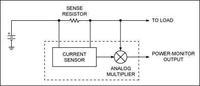
Figure 1. In this design the MAX4211 multiplies load current and load voltage to provide an analog output voltage proportional to the power consumed by a load.
Alternate Use of Analog Multipliers in High-Side Current-Sense Amplifiers
There is another way to use the analog multiplier. Instead of connecting the analog multiplier's external input to the voltage of the load, connect it to the ADC's external reference voltage. In this design the analog multiplier is not measuring power, but is relating the voltage output of the current-sense amplifier to the ADC's reference voltage.
Figure 2 shows this application where the MAX4211 measures the battery charge and discharge currents. The voltage output, POUT, is fed to a 16-bit ADC with an input voltage range from 0 to VREF. Here VREF is provided by an external voltage regulator and should be between 1.2V and 3.8V (3.8V in this application example). The analog multiplier input accepts a voltage between 0 and 1V, so the two resistors, R1 and R2, divide the 3.8V reference voltage. Assuming that R2 = 1kΩ and R1 = 2.8kΩ, then VIN = 1V. The MAX4211 has gain of 25 and a sense voltage range (VSENSE) from 0 to 150mV, which produces an output voltage at both POUT and IOUT between 0 and 3.75V (proportional to the current that flows on the load).

Figure 3 shows the same application with an ADC that has an internal voltage reference. The application presented here applies when the ADC's voltage reference is either internal or external.

Figure 3. In this design the MAX4211 uses an ADC with internal reference voltage to measure the battery charge and discharge currents.
There is an advantage to using the POUT output of the current-sense amplifier instead of the IOUT output: the signal fed to the ADC (which is proportional to the current in the load) is scaled by the VREF voltage. Note also, that using the POUT output can relax the accuracy requirements demanded by the voltage reference. This relaxed demand on the voltage reference happens because the digital code produced by the ADC depends on the ratio between its input signal and its reference voltage (which represents the full-scale value). The POUT output is a direct function of the reference voltage, therefore the ADC measurement is, in principle, independent of the accuracy of the reference voltage.
If the IOUT were connected to the ADC, however, then the ADC would see any errors in the reference voltage as a full-scale error. The two equations below represent the ratio of ADC input to ADC full-scale, and illustrate this concept:
POUT/VREF = ILOAD × RSENSE × 25 × VREF × R2/(R1 + R2)/VREF =
ILOAD × RSENSE × 25 × R2/(R1 + R2)
IOUT/VREF = ILOAD × RSENSE × 25/VREF
Equation 1, which uses the POUT output, is not dependant on the accuracy of VREF. Equation 2, which uses the IOUT output, produces an error that is the inverse function of the VREF accuracy.
The overall accuracy of the system shown in Figures 2 and 3 depends on many factors: resistor tolerance, the amplifier's gain error, voltage offset and bias current, reference voltage accuracy, ADC errors, and the drift versus temperature of all the above. The solution presented in Figures 2 and 3 uses the analog multiplier of the MAX4211 to improve the system accuracy by eliminating one of the causes of errors—the inaccuracy of the reference voltage.
There are at least three sources of errors that can affect VREF accuracy:
- Initial DC error (percentage of the nominal value)
- The VREF value changes with the load
- VREF value changes over temperature
Figure 4 illustrates the second error source listed above: a heavy load is connected to VREF and its value drops from 3.8V to 1.2V when the load is increased. POUT matches the VREF drop profile and changes accordingly.

Figure 4. Data illustrate how VREF changes with the load. Here POUT/IOUT vs. VREF with VSENSE = 125mV.
The following Figures 5, 6 and 7 show VREF and the MAX4211's outputs changing with temperature. Here VSENSE is kept constant at 100mV and VCC is 5V. The temperature of the circuit for Figure 2 varies from -40°C to +85°C (with intermediate steps at -20°C, 0°C, +25°C, +45°C and +65°C). Figure 5 shows the profile of VIN over temperature (as a consequence of VREF's drift over temperature).

Figure 5. VIN vs. temperature.
Figure 6 shows the profile of the MAX4211's IOUT versus the ratio of IOUT/VIN, which is proportional to the ADC's input-signal/full-scale ratio (in the hypothetical case where the ADC was driven by IOUT).
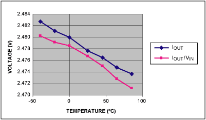
Figure 6. IOUT vs. IOUT/VIN with VSENSE = 100mV.
It is very evident that the IOUT/VIN ratio is dependent on the VIN profile of Figure 5. The dip between 0°C and +45°C of VIN in Figure 5 is reflected as a hump around the same temperature range in the IOUT/VIN profile of Figure 6. The ADC measurement is affected by the changes of the voltage reference, VREF, with the temperature.
Finally, Figure 7 shows the profile of the MAX4211's POUT versus the ratio of POUT/VIN. Again, POUT/VIN is proportional to the ADC's input-signal/full-scale ratio.
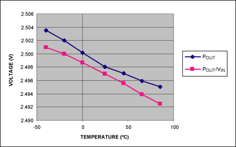
Figure 7. POUT vs. POUT/VIN with VSENSE = 100mV.
Figure 7 shows how the ratio of POUT/VIN is independent from the VIN profile over temperature that is shown in Figure 5. The drop of VIN between 0°C and +45°C is already "absorbed" by the POUT output and does not appear in the POUT/VIN ratio. The ADC measurement does not depend on the VREF profile over temperature.
Figure 8 summarizes these concepts by showing both IOUT/VIN and POUT/VIN together with their ideal linear trend lines.

Figure 8. POUT/VIN vs. IOUT/VIN with VSENSE = 100mV.
Conclusion
The integrated analog multiplier of high-side current-sense amplifiers is typically used to measure the power at the load. There is, however, another possible application for this integrated multiplier. The current-sense amplifier can be connected to an ADC that uses either an internal or an external voltage reference. In both cases, the overall accuracy of the measurement strongly depends on the accuracy of the voltage reference (VREF). By multiplying the load current measurement with VREF, the overall accuracy of the ADC measurement is no longer dependent on voltage reference errors. Using this alternate design, one can improve measurement accuracy even in the presence of a low-cost and less-accurate voltage reference.
A similar article appeared on the ED website on March 26, 2008.


