10µA Quiescent Current Step-Down Regulator Extends Standby Time in Handheld Electronics
10µA Quiescent Current Step-Down Regulator Extends Standby Time in Handheld Electronics
by
Greg Dittmer
Feb 1 2000
Introduction
Many handheld products on the market today are used only occasionally but must be kept alive and ready all the time. When not being used, the circuitry is powered down to save battery energy, with a minimum amount of circuitry remaining on. Although the supply current is significantly reduced in this low power standby mode, the battery energy will still be slowly depleted to power the keep-alive circuitry and the regulator. If the device spends most of its time in this standby mode, the quiescent current of the regulator can have a significant effect on the life of the battery (see Figure 1). To maximize the life of the battery in these types of products, Analog Devices has extended its family of low quiescent current step-down converters. The LTC1474/LTC1475 series broke new ground a few years ago by providing a monolithic step-down regulator that requires only 10µA of supply current to regulate its output voltage at no load while maintaining high efficiency at loads up to 300mA. Now, two new products provide solutions for applications requiring higher output currents or constant-frequency operation at a higher switching frequency while still operating on the ultralow 10µA no-load supply current. The new LTC1771 is a constant off-time controller for up to 5A of output current with the addition of an appropriately sized external P-channel FET. A second product, soon to be released, is a monolithic regulator that provides constant frequency (550kHz) plus synchronous operation at up to 500mA of output current.
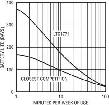
Figure 1. 9V battery-life comparison for load requiring 100mA normal and 100µA standby current at 3.3V.
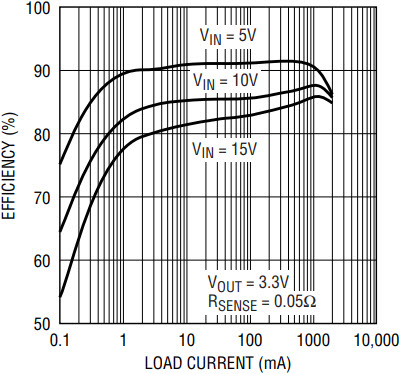
Figure 2. LTC1771 efficiency vs load current for Figure 5’s circuit.
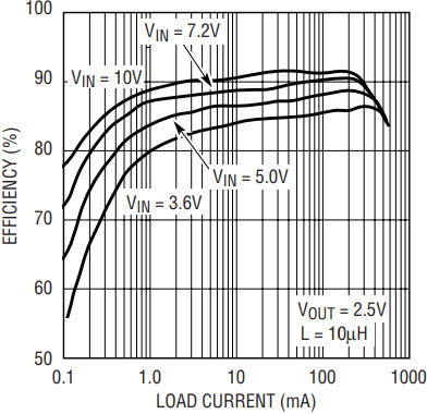
Figure 3. Efficiency vs load current for a new constant frequency monolithic regulator.
LTC1771 Controller for Output Loads to 5A
The LTC1771 is a step-down controller that drives an external P-channel MOSFET for output loads up to 5A. Its low quiescent current and flexible operation with a wide range of output loads allow the LTC1771 to maintain high efficiency for over four decades of operating current. Wide supply range (2.8V–18V) and 100% duty cycle for low dropout allow maximum energy to be extracted from the battery, while current mode operation gives excellent transient response and startup behavior. LTC1771 also features short-circuit protection (the maximum current is programmable with an external sense resistor), micropower shutdown to 2µA and a Burst Mode disable pin for low noise applications.
The LTC1771 uses a constant off-time, current mode architecture to regulate its output voltage. During normal operation, the P-channel MOSFET is turned on at the beginning of each cycle, causing current to ramp up in the inductor and sense resistor. When the sensed current reaches the current comparator threshold, the current comparator trips and triggers a 1-shot timer that turns off the MOSFET for 3.5µs. At the end of this period, the MOSFET is turned back on and the cycle is repeated. The peak inductor current at which the current comparator trips is controlled by the voltage on pin 2 (ITH), the output of the error amplifier. An external resistor divider allows the error amplifier to receive an output feedback voltage. When the load current increases, it causes a slight decrease in the feedback voltage, which, in turn, causes the average inductor current to increase until it matches the new load current.
Burst Mode for Outstanding Low Current Efficiency
The LTC1771 is able to maintain an ultralow no-load supply current and high efficiency at extremely light loads by using Burst Mode operation. Burst Mode operation commences when the load, detected by a comparator monitoring the ITH voltage, falls below about 20%–30% of the maximum load. During Burst Mode operation, short burst cycles of normal switching to charge the output capacitor alternate with longer sleep periods when the switch is turned off and the load current is supplied by the output capacitor. During this sleep period, only the minimum required circuitry—the reference voltage and the error amplifier—are left on. Supply current is further reduced with innovative new circuitry that allows the error amplifier to run on 10% of its normal operating current during sleep mode with no degradation in the transient response, reducing the total supply current to less than 10µA. At light loads, the regulator spends most of the time in this low quiescent current sleep mode, minimizing supply current and maximizing efficiency.
Burst Mode operation can be disabled by pulling the Mode pin to ground. Disabling Burst Mode operation allows the loads to decrease another decade, to about 1%–2% of maximum load, before the regulator must skip cycles to maintain regulation. Although less efficient, disabling Burst Mode operation is useful because it reduces both audio and RF interference by reducing voltage and current ripple and by keeping operating frequency constant at lower output currents.
Component Considerations for Minimizing Supply Current
No-load supply current for the LTC1771 consists of the 10µA quiescent current of the IC plus a small additional current to power the low frequency burst cycles needed to recharge the output capacitor. Even at no load, the output capacitor is slowly discharged due to leakage currents from the feedback resistors and the Schottky diode. This leakage current, though small, can be significant when the total supply current is only 10µA. The feedback resistor leakage can be minimized by using resistors in the megohm range. Care must be used in selecting the Schottky diode to minimize no-load supply current without sacrificing efficiency at higher loads. Low leakage is critical for minimizing no-load supply current; however, forward voltage drop is critical for higher current efficiency because loss is proportional to the forward voltage drop. Unfortunately, these are conflicting parameters (see Figure 4) and the user will need to weight the importance of each spec in choosing the best diode for the application.
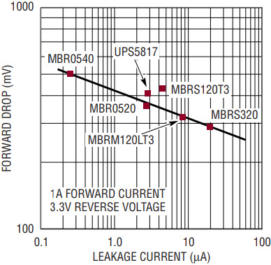
Figure 4. Schottky diode parameter trade-off.
3.3V/2A Step-Down Regulator
A typical application circuit using the LTC1771 is shown in Figure 5, with the associated efficiency curves in Figure 2. This circuit supplies a 2A load at 3.3V with an input supply range of 4.5V to 18V. The 0.05Ω sense resistor sets the maximum output current to just above 2A. The 15µH inductor sets the inductor ripple current at about 1A, and with the 0.05Ω ESR of the output capacitor, results in 50mV of output voltage ripple. Since the LTC1771 gate drive pin swings rail-to-rail, a MOSFET must be chosen that can handle the full supply voltage. The Si6447 P-Channel MOSFET is a good compromise between low gate charge and RDS(ON). Gate charge affects efficiency at lighter loads, whereas RDS(ON) affects the efficiency at heavier loads. The 4.5V minimum supply voltage is due to minimum gate voltage required for the Si6447. If the input supply is limited to 12V or less, a 2.5V MOSFET, such as the Si3443, could be used allowing the regulator to operate to lower supply voltages. The Microsemi Powermite UPS5817 Schottky diode (617-926-0404) provides a good compromise between reverse leakage and forward drop for the 1A–2A range. The diode leakage and the feedback resistors increase the no-load supply current to about 12µA.
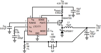
Figure 5. LTC1771 3.2V/2A regulator.
Conclusion
With Analog Devices' growing family of high performance 10µA parts, the designers of handheld electronics now have a myriad of solutions to optimize their designs without compromising the main goals of extending standby time and maximizing battery live. With these parts, the designer has a choice of high or low input voltage and monolithic or controller configurations. The LTC1771 provides a wide supply range up to 18V and output currents up to 5A, whereas an upcoming product gives you constant frequency operation and loads of up to 500mA without the need for an external MOSFET and Schottky diode. With both available in the MS8 package and requiring only 10µA of supply current at no load, these products are perfect solutions for handheld electronics.


