


Overview
Design Resources
Description
The MAXREFDES1269 demonstrates how to build a DC-DC buck converter using the MAX20098 step-down controller for 5V DC output applications from a 6V to 36V input. This reference design delivers up to 20A at 5V output. The design uses a six-layer board. Table above shows an overview of the design specification.
The MAX20098 is a 3.5V to 36V synchronous, step-down DC-DC controller. It uses a current-mode control architecture and can operate in the pulse-width modulation (PWM) or skip-mode control schemes. The device can operate in dropout conditions at a 99% duty cycle. The external sync pin (FSYNC) logic input, under light-load applications, allows the device to operate either in the skip-mode or fixed-frequency forced-PWM (FPWM) mode to minimize electromagnetic interference (EMI). The output voltage is programmable from 1V to 10V with fixed 3.3V/5V options. The feedback (FB) regulation is accurate within ±1% over -40°C to +125°C.
Features & Benefits
- Efficiency = 88% at Full Load
- Output-Voltage Ripple < 50mV across Line and Load Conditions
- Overshoot < 150mV for 50% Load Step
- Continuous Conduction Mode (CCM) Operation
- Internal Soft-Start
- Overall Solution Size = 572mm2
Parts Used
Details Section
The MAXREFDES1269 demonstrates how to build a DC-DC buck converter using the MAX20098 step-down controller for 5V DC output applications from a 6V to 36V input. This reference design delivers up to 20A at 5V output. The design uses a six-layer board. Table 1 shows an overview of the design specification.
The MAX20098 is a 3.5V to 36V synchronous, step-down DC-DC controller. It uses a current-mode control architecture and can operate in the pulse-width modulation (PWM) or skip-mode control schemes. The device can operate in dropout conditions at a 99% duty cycle. The external sync pin (FSYNC) logic input, under light-load applications, allows the device to operate either in the skip-mode or fixed-frequency forced-PWM (FPWM) mode to minimize electromagnetic interference (EMI). The output voltage is programmable from 1V to 10V with fixed 3.3V/5V options. The feedback (FB) regulation is accurate within ±1% over -40°C to +125°C.
A small-size, high-efficiency, synchronous step-down converter using the MAX20098 is demonstrated for a 5V/20A application. Table 1 provides an overview of the design specification. Measured data and waveforms from the hardware setup are found in the test results.
| Parameter | Symbol | Min | Typ | Max |
| Input Voltage | VIN | 6V | 14V | 36V |
| Frequency | fSW | 400kHz | ||
| Efficiency | η | > 85% | ||
| Output Voltage | VOUT | 5V | ||
| Load Step | ISTEP | 10A to 20A | ||
| Transient Deviation | ΔVOUT | 150mV | ||
| Output Voltage Ripple | VPK-PK | 50mV | ||
| Output Current | IOUT | 0A | — | 20A |
| Output Power | POUT | 100W | ||
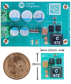
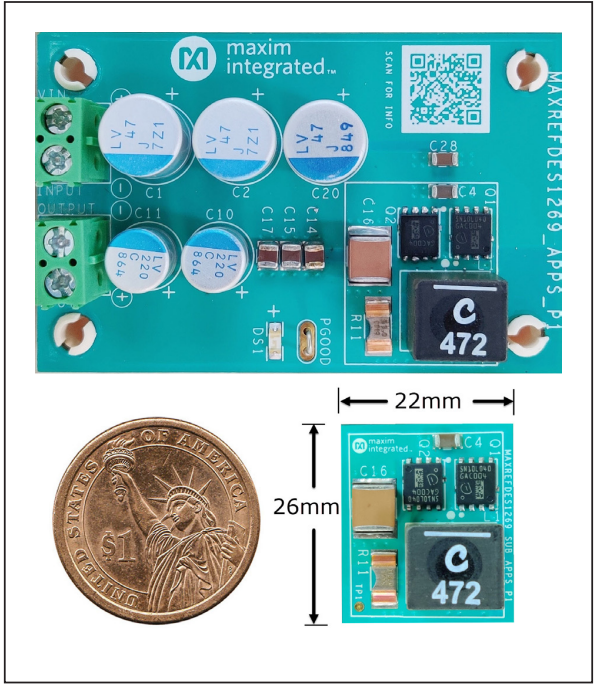
This document describes the hardware in Figure 1. It provides a detailed, systematic technical guide to design a buck converter using the MAX20098 for high voltage and smaller size. The small board in Figure 1 shows the actual solution size. Refer to the MAX20098 and MAX20098 EV kit data sheets for device operation details. The power supply was built and tested. The details follow later in this document.
Required Equipment
- AC-DC power supply: Chroma Systems 62015L-60-6
- Electronic load: Keithley® 2380-120-60
- Oscilloscope: Teledyne® LeCroy® WaveSurfer® 3024z
- Multimeter: Keithley DMM6500
Procedure
The reference design is fully assembled and tested. Follow these steps to verify the board operation:
- Connect the positive and negative terminals of the power supply to the input connector.
- Set the power-supply voltage to 14V and current limit to 20A.
- Turn on the power supply.
- Verify that VOUT is close to 5V using the DMM.
- Verify that the switching frequency is close to 400kHz by monitoring the switching node voltage with the oscilloscope.
Design Procedure for a High-Efficiency Buck Converter
The design process is divided into the following stages:
- Calculating the switching frequency resistor
- Selecting the output voltage
- Selecting the current-sense resistor
- Selecting the inductor
- Selecting the input capacitor
- Selecting the output capacitor
- Selecting the external MOSFET
- Compensation network
- Selecting the BIAS capacitor
- PCB layout guidelines
This document complements the information in the MAX20098 data sheet.
The following design parameters are used throughout this document:
- VIN = Input voltage
- VOUT = Output voltage
- IOUT = Output current
- fSW = Switching frequency
- D = Duty cycle
Step 1. Calculating the Switching Frequency Resistor
The switching frequency (fSW) is set by a resistor (R1) connected from the FOSC pin to the AGND pin. The R1 value is:
Set R1 = 66.5kΩ for a switching frequency of 400kHz.
Step 2. Selecting the Output Voltage
Set the output voltage using the R15 and R16 resistors. VFB is the internal reference voltage and its typical value is 1V.
Setting VOUT = 5V and VFB = 1V (typ):
where R16 = 10kΩ, which gives R15 = 40.2kΩ.
Step 3. Selecting the Current-Sense Resistor
Use a ±1% tolerance current-sense resistor between the inductor and output for the best current-sense accuracy and overcurrent protection. This configuration constantly monitors the inductor current, allowing accurate current-limit protection. The overcurrent protection is enabled at 20% higher than the peak current of the inductor:
where VLIMIT is 71mV, which is the minimum value of the current-limit threshold from the MAX20098 data sheet.
ΔIP-P is considered as 4A. A margin of 15% is considered for the output current protection. R11 is calculated as 2.81mΩ. A Bourns CSS2H-2512K-3L00F 3mΩ metal element was chosen as the current-sense resistor.
An RC circuit is added across the sense resistor for noise filtering on the current-sense signal. RC is chosen for a 1/10 time constant compared to the switching time. R22 = 47Ω and C25 = 1nF.
Step 4. Selecting the Inductor
The inductor is selected based on the LIR and slope compensation. The LIR is the ratio of the peak-to-peak inductor current ripple to the average value of the inductor current. Typically, an inductor value is chosen to produce a current ripple (ΔIL) equal to 30% of load current, giving a LIR of 0.3.
The inductance value required to meet the current ripple:
The inductance value required to meet the slope compensation:
where m is the internal slope compensation, AVCS is the current-sense gain (13V/V), and RCS is the current-sense resistor value.
The inductance value to meet both the equations:
The required value of inductance is 2.71µH.
Additionally, ensure the following relationships are satisfied:
and
where
and
and
The Coilcraft® XAL1010-472ME with a 4.7µH inductance, and 25.4A ILSAT and 24A ILRMS saturation current is chosen.
Step 5. Selecting the Input Capacitor
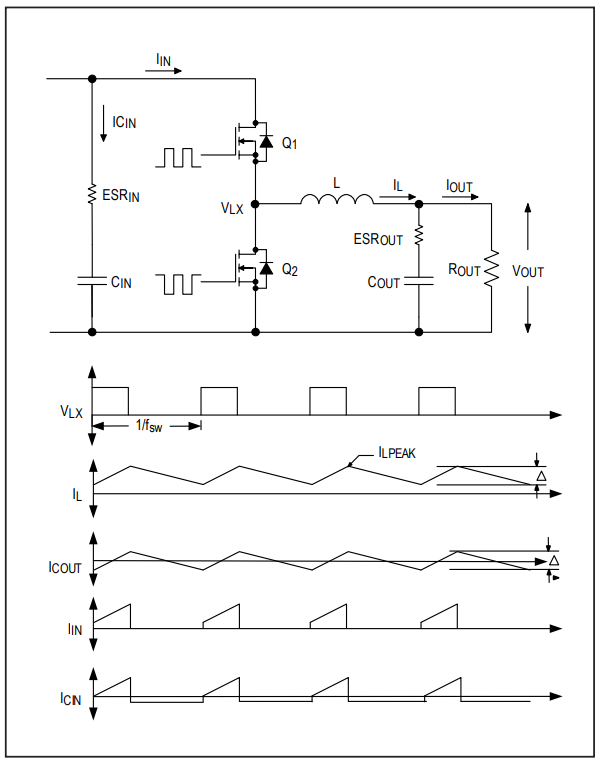
The input capacitor RMS current requirement (IRMS) is defined as:
where IOUT(MAX) is the maximum load current. IRMS has a maximum value when the input voltage equals twice the output voltage (VIN = 2 x VOUT). So, IRMS = IOUT(MAX)/2. The required RMS current rating of the input capacitor is 10A.
The input-voltage ripple is composed of ΔVQ (caused by the capacitor discharge) and ΔVESR (caused by the ESR of the input capacitor). The following equations show the ESR and capacitor requirement for a target voltage ripple at the input:
IOUT is the maximum output current in amps, ΔIP-P is the peak-to-peak inductor current in amps, and fSW is the switching frequency. The input capacitor is designed for an input voltage ripple of 3%. ΔVESR is the input voltage ripple due to ESR, which is 0.054V. ΔVQ is the input voltage ripple caused by the capacitor discharge, which is 0.126V. Here, ESRIN = 2.2mΩ and CIN = 99µF. Some margin must be reserved due to the capacitor’s DC bias and temperature characteristics. A combination of ceramic and electrolytic capacitors is used. Electrolytic capacitance = 3 × 47µF and ceramic capacitance = 2 × 4.7µF meet both the capacitance and RMS current requirements.
Step 6. Selecting the Output Capacitor
The required ESR and capacitance value due to load transient are:
ISTEP is the load step current in amps. The output capacitor is designed for an output voltage overshoot of 3% for a 50% load change. ΔVESR is the output voltage overshoot due to ESR, which is 0.045V. ΔVQ is the output voltage overshoot caused by the capacitor discharge, which is 0.105V. Here, ESROUT = 4.5mΩ and COUT = 315µF. Some margin must be reserved due to the capacitor’s DC bias and temperature characteristics. A combination of ceramic and electrolytic capacitors is used. Electrolytic capacitance = 2 × 220µF and ceramic capacitance = 5 × 4.7µF + 100 µF. A higher value of capacitance is used at the output to create the point-of-load application.
The output voltage ripple due to the ESR and capacitance are:
where ΔIP-P is the peak-to-peak inductor current in amps and fSW is the switching frequency. ΔVESR is calculated as 1.5mV and ΔVQ is 2mV. So, the total output voltage ripple is 3.5mV, which is within the specified limit of 50mV.
Step 7. Selecting the External MOSFET
Two external MOSFETs are required for the buck architecture supported by the MAX20098. The MOSFETs must be selected based on the critical parameters such as on-resistance, breakdown voltage, output capacitance, and input capacitance. A low RDSON reduces the conduction losses in the MOSFET and a small gate/output capacitance reduces the switching losses.
Typically, a lower RDSON MOSFET has higher gate charge for the same breakdown voltage. Hence, a compromise is made depending on the conditions to which the MOSFET is subjected. The Infineon® IAUC100N10S5L040 n-channel, 100V MOSFETs were selected here. This MOSFET has a very low RDSON of 4mΩ and gate charge of 60nC to ensure higher efficiency for the converter.
Step 8. Compensation Network
The IC uses the current-mode control scheme for a buck controller. A series resistor (R2) and a capacitor (C5) are used for a stable, high-bandwidth loop in applications where ceramic capacitors are used for output filtering. The frequency of the zero created by the capacitance and ESR is lower than the desired closed-loop crossover frequency for other types of capacitors due to the higher capacitance and ESR. Add another compensation capacitor (C7) from COMP to AGND to cancel this zero to stabilize a non-ceramic output-capacitor loop.
R2 = 68kΩ, C5 = 2.7nF, and C7 = 10pF were the chosen values. An additional RC circuit was added across the top feedback resistor to boost the phase margin. R17 = 2.7kΩ and C24 = 330pF were the selected values.
Step 9. Selecting the BIAS capacitor
The internal circuitry of the IC requires a 5V bias supply. An internal 5V linear regulator (BIAS) generated this supply. The BIAS pin is bypassed with two 2.2µF ceramic capacitors in parallel to guarantee stability under full load.
Step 10. PCB Layout Guidelines
A good PCB layout is critical to achieve low switching power losses, and a clean, stable operation. Use a multilayer board for better noise immunity. Follow the guidelines for a good PCB layout:
- All the connections carrying pulsed currents must be very short and as wide as possible. The inductance of these connections must be kept to an absolute minimum due to the high di/dt of the currents. The inductance of a current-carrying loop is proportional to the area enclosed by the loop. The inductance is reduced if the loop area is made very small. Also, small current loop areas reduce the radiated EMI.
- A ceramic input filter capacitor must be placed close to the IC’s VIN pins. Also, its ground loop to the PGND must be short. This eliminates as much trace inductance effects as possible and gives the IC a cleaner voltage supply. A bypass capacitor for the VCC pin also must be placed close to the pin to reduce the effects of trace impedance. Its ground loop to the PGND must be short.
- The analog small-signal ground and power ground for switching currents must be kept separate when routing circuitry around the IC. They must be connected where switching activity is minimal, typically the return terminal of the VCC bypass capacitor. Doing so keeps the analog ground quiet. The ground plane must be kept continuous and unbroken as far as possible. No trace-carrying, high-switching current must be placed directly over any ground plane discontinuity.
- The PCB layout also affects the thermal performance of the design. A few thermal vias that connect to a large ground plane must be provided under the IC’s exposed pad to dissipate heat efficiently. The PCB size, copper thickness, and board layer numbers affect the temperature dissipation capacity of the board. It can support a 10A load current with 1oz of copper, six layers, and an 88mm x 45mm board for this reference design.
Documentation & Resources
-
MAXREFDES1269 Design Files3/3/2021ZIP1 M
-
MAXREFDES1269: 5V/20A, Synchronous Step-Down Converter Using the MAX200983/3/2021PDF615 K
Support & Training
Search our knowledge base for answers to your technical questions. Our dedicated team of Applications Engineers are also available to answer your technical questions.