
MAXREFDES1202


Overview
Design Resources
Description
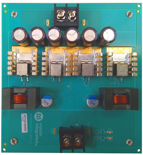
The MAXREFDES1202 is a dual-phase, buck converter reference design developed using the MAX17558, MAX15019A, and MAX17552. This reference design is rated to operate over a wide input voltage range from 15V to 55V. The design can deliver an output power of 360W at 12V.Features & Benefits
- Very High Efficiency > 95% at Full Load
- Very Low Line Regulation < 0.1% and Very Low Load Regulation < 0.25%
- Inductor DCR Current Sensing
- Output-Voltage Ripple < 0.5% at VIN (nom)
- Overshoot < 3% for 50% Step Load
Parts Used
Details Section
The MAXREFDES1202 is a dual-phase, buck converter reference design developed using the MAX17558, MAX15019A, and MAX17552. This reference design is rated to operate over a wide input voltage range from 15V to 55V. The design can deliver an output power of 360W at 12V.
Main features include the following:
- Very High Efficiency > 95% at Full Load
- Very Low Line Regulation < 0.1% and Very Low Load Regulation < 0.25%
- Inductor DCR Current Sensing
- Output-Voltage Ripple < 0.5% at VIN (nom)
- Overshoot < 3% for 50% Step Load
A single-output, dual-phase buck converter is demonstrated for a 15V to 55V input voltage range application. The output is 12V, delivering 30A of current at full load.
The MAX17558 is used for controlling the converter. This IC is a dual-output, synchronous step-down controller using a constant-frequency, peak-current-mode architecture. It has wide input supply range of 4.5V to 60V. The device also provides the ability to run two controllers 180° out of phase to reduce power loss and noise due to the input-capacitor ESR.
The gate pulses from the MAX17558 are input to the MAX15019A gate driver, which is used for driving the MOSFETs. The MAX15019A is a high-frequency, 125V half-bridge, n-channel MOSFET driver that drives high and low-side MOSFETs. This IC supports supply voltages from 8V to 12.6V VDD, thus making it suitable for driving MOSFETs with higher gate threshold voltage.
The power supply for the gate driver is derived from the MAX17552 low-cost, high-voltage buck controller IC.
Table 1 shows an overview of the design specification.
| Parameter | Symbol | Min | Typ | Max |
| Input Voltage | VIN | 15 | 48 | 55 |
| Output Voltage | VO | 12V | ||
| Load Current | IO | 30A | ||
| Frequency | fSW | 100kHz | ||
| Efficiency at Full Load | η | >90% | ||
| Efficiency at Full Load | ΔVO_OS | 5% | ||
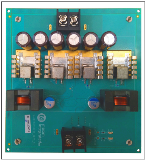
This document describes the hardware shown in Figure 1. It provides a detailed, systematic technical guide for designing a dual-phase buck converter using the MAX17558 currentmode controller. This power supply has been built and tested, details of which follow later in this document.
Required Equipment
- DC Power Supply
- DC Electronic Load
- Multimeter
- Oscilloscope
Procedure
This reference design is fully assembled and tested. Follow these steps to verify board operation:
- Connect a 60V DC power supply to the input.
- Keep the input voltage at 48V and turn on.
- Observe the output voltage using a multimeter. It should show 12V.
- Connect a DC electronic load at the output and load in steps up to 30A. Observe the output-voltage regulation and output ripple.
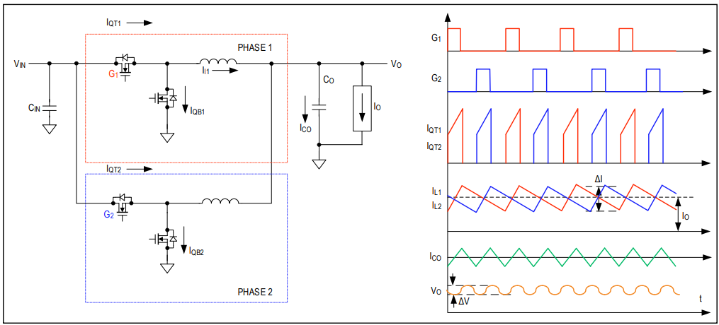
Figure 2 shows the electrical block diagram of a dualphase buck converter. The two phases share a common input and load. Current delivered to the load is shared equally by the inductors and switches. Each phase is operated with 180° phase difference between the PWM gate signals for improved ripple performance.
Compared to single-phase buck regulators, a dual-phase buck converter offers several advantages as follows:
- Load Sharing
- Input Ripple Reduction
- Output Ripple Reduction
As seen in Figure 2, the two phases are operated at a 180° phase shift. G1 and G2 are the gate signals applied to the top switches of their respective phases. IL1 and IL2 are the inductor currents, IQT1 and IQT2 are the top switch currents, and ICO is the output capacitor current.
Assuming that the current drawn from the input supply is DC, the AC of the switch currents IQT1 and IQT2 is supplied by the input capacitor. The phase shift of the two switch currents effectively reduces the peak of the input current by half, while the frequency is doubled.
Similarly, the inductor currents IL1 and IL2 supply the load. A 180° phase shift between the two phases causes a reduced ripple current (ICO) in the output capacitor.
Inductor
The required inductance per phase is calculated based on the inductor ripple current ratio (LIR). This is defined as the ratio of the peak-to-peak inductor current (ΔIL) to the average current (IO). For a switching frequency:

and operating at a minimum duty cycle:

and

the inductance required per phase is calculated by applying volt-second balance on the inductor voltage as follows:

With LIR at 0.4 and the load current at 15A (per phase current), the value of inductance is calculated. Based on the calculated specifications for the inductors, the Coilcraft® VER2923-153KL was selected.

The losses in the inductor have two components: copper loss and core loss. The core loss is obtained from the manufacturer website. The copper loss is calculated as follows:
Inductor copper loss = IL—RMS2 × RCS
where:

RCS is the DC resistance (DCR) of the inductor. DCR is used for current sensing in this reference design.
RCS = 2.6mΩ
Table 2 gives a summary of the calculated values for power loss in each inductor.
| Parameter | Symbol | Value | Units |
| Inductor Ripple Current Ratio | LIR | 0.4 | — |
| Peak-to-Peak Inductor Ripple | ΔIL | 6.0 | A |
| Duty Cycle at VGNOM | D | 0.25 | — |
| Inductor RMS Current at Full Load | IL-RMS | 15.10 | A |
| Inductor Cu Loss per Phase | PIND-CU | 0.59 | W |
| Inductor Core and AC Losses (approx.) per Phase | PIND-AC | 1 | W |
Current Sensing
An inductor DCR is used for current sensing in this design. This effectively reduces the losses associated with two current shunt resistors, leading to improved efficiency. The voltage across the inductor is conditioned to obtain the current signal.
Figure 3 shows the DCR current-sensing circuit. An RC low-pass filter is connected across the inductor, which has a DC resistance of RCS.
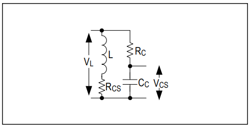
The equations relating the current through the inductor and voltage developed across the inductor can be written in the Laplace domain as follows:

having:

The sensed voltage (VCS) is a simple gain multiplied by the inductor current (IL), VCS = RCSIL(s), and the values are RC = 17.4kΩ and CC = 330nF.
Table 3 gives the values of current-sense signal (VCS) for the full load current at a nominal input voltage of 48V.
| Parameter | Symbol | Value | Units |
| DCR Resistance | RCS | 2.6 | mΩ |
| Peak Inductor Current | IP | 18 | A |
| Measured Sense Signal | VCS | 46.8 | mV |
| Current-Sense Limit | VLIM | 75 | mV |
| Current-Sense Amplifier Gain | GCS | 13.3 | — |
MOSFETs
The current and voltage waveforms in the synchronous switches during on and off period are shown in Figure 4a for one phase. The on-state losses are due to a resistive drop in the MOSFETs.
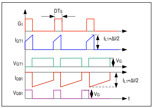
The RMS current and the conduction power loss (PT—CONDN) in the top device of a phase are given by the following equations:

PT—CONDN = IQT1 RMS2 x RRDS—ON
Figure 4b shows the turn-on and turn-off transients in the MOSFET. ID is the drain current and VDS is the drain-tosource voltage of the MOSFET. The switching loss (PT-SW) during turn-on and turn-off transients and the gate charging loss (PT-GATE) are calculated as follows:
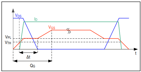
PT—SW = f SWVINI1∆t
PT—GATE = QGVDRIVEfSW
The total power losses (PT) in the top MOSFET per phase are calculated as follows:
PT = PT—CONDN + PT—SW + PT—GATE
Refer to the BOM in the Design Resources tab for the components chosen.
| Parameter | Symbol | Value | Units |
| Drain-to-Source Resistance | RDS-ON | 2.0 | mΩ |
| RMS Current of Top MOSFET | IQT1-RMS | 7.55 | A |
| Conduction Loss | PT-CONDN | 0.148 | W |
| Turn-On Time | Δt | 26 | ns |
| Switching Loss | PT_SW | 1.8 | W |
| Gate Loss | QG | 168 | nC |
| Gate Drive Loss | PT_GATE | 0.168 | W |
The RMS current IQB1-RMS and on-state conduction losses (PB-CONDN) in the bottom device are given by the following equations:

PB—CONDN = IQB1—RMS2 x RRDS—ON
During dead times (when DH is falling and DL is rising or when DL is falling and DH is rising), the body diode of the lower MOSFET conducts to maintain current through the inductor. This can be termed as “dead-time loss” (PB-DT). Also, when the top MOSFET is turning on, the body diode of the lower MOSFET recovers to the blocking state, leading to reverse-recovery losses (PRR) in the device.

PRR = QRRVINfSW
Table 5 shows the summary of losses in the bottom MOSFET.
| Parameter | Symbol | Value | Units |
| Drain-to-Source Resistance | RDS-ON | 2.0 | mΩ |
| RMS Current of Top MOSFET | IQB1-RMS | 13.1 | A |
| Conduction Loss | PB-CONDN | 0.342 | W |
| Dead Time | ΔtD | 40 | ns |
| MOSFET Diode Drop | VF | 0.9 | V |
| Dead-Time Loss | PB-DT | 0.054 | W |
| Gate Drive Loss | PB-B_GATE | 0.168 | W |
| Reverse-Recovery Charge | QRR | 287 | nC |
| Reverse-Recovery Loss | PRR | 1.3776 | W |
Output Capacitor
Figure 5 shows the current in the two inductors and in the output capacitor when operating in full load at a nominal input voltage. The capacitor sees the ripple current at twice the switching frequency of the inductor current.
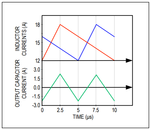
The ratio of the peak-to-peak capacitor ripple current to the inductor ripple current is around 0.75 at duty cycle of 0.25. The RMS current through the output capacitor is calculated as follows:

The output capacitance (COUT) depends on the desired steady-state voltage ripple and voltage overshoot specification. The steady-state ripple (ΔVO_SS) has 2 components: one due to drop in actual capacitance (ΔVO_Q) and another due to drop in ESR of the capacitor (ΔVO_ESR).
ΔVO_SS = ΔVO_ESR + ΔVO_Q
For ceramic capacitors, ΔVO_Q predominates. For electrolytic capacitors, the ΔVO_ESR component predominates.
For a steady-state ripple of ΔVO_SS, the desired output capacitance is calculated from the following equations:

For achieving good transient performance, the required output capacitance is calculated as:

where ΔIO is the total load change, fC is the unity gain bandwidth (or crossover frequency), and ΔVO_OS is the transient overshoot specification.
A combination of electrolytic and ceramic capacitors has been used for optimal performance in this design. Table 6 shows the summary of current and loss in the output capacitor.
| Parameter | Symbol | Value | Units |
| Peak-to-Peak Inductor Ripple | ΔIL | 6.0 | A |
| Peak-to-Peak Capacitor Ripple Current | ΔIC | 4.5 | A |
| Capacitor RMS Current | ICO_RMS | 1.3 | A |
| Total Output Capacitance | COUT | 833 | µF |
| Effective Series Resistance | ESR | 14 | mΩ |
| Power Loss | PCO | 2.73 | mW |
Input Capacitor
The input filter capacitor reduces the peak currents drawn from the power source and reduces noise and voltage ripple on the input caused by the circuit’s switching.
Figure 6 illustrates the current flowing through the switch and input capacitor during rated operating voltage and current. For a DC current drawn from the input (IIN = DIO), the RMS current flowing through the input capacitor for a single-phase buck converter is given as:
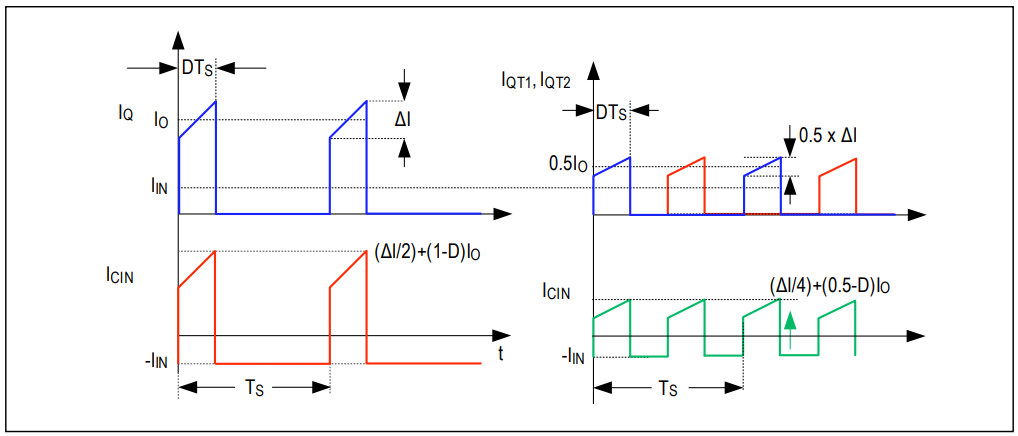

The RMS of the current in input capacitor for a dual-phase buck converter under nominal operating conditions (D < 0.5) is given as:

| Parameter | Symbol | Value | Units |
| Input Capacitance RMS Current for Single-Phase Buck Converter | ICIN-RMS-1PH | 13.33 | A |
| Input Capacitance RMS Current for Dual-Phase Buck Converter | ICIN-RMS-2PH | 10.8 | A |
Compensation
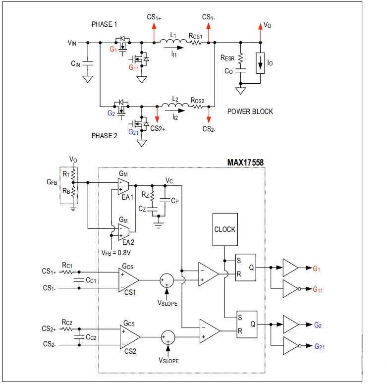
Figure 7 shows the control block diagram of a dual-phase buck converter. The output-voltage error amplifier of both phases operates in parallel to derive a single control signal (VC). Here, GCS is the current-sense amplifier gain, GM is the internal transconductance error amplifier gain, and GFB is the output-voltage feedback divider gain (0.8/output voltage).
The plant transfer function consists of the pole fP1 formed by the load and output capacitor:

An additional zero (fZ1) is introduced by the output capacitor ESR:

The voltage error amplifier transfer function introduces one zero and two poles.
The crossover frequency is kept at 1/10th of the switching frequency fSW, and RZ is calculated from the following:

CZ is calculated by placing the compensator zero near the system pole fP1:

CP is calculated by placing the compensator pole near fZ1, or half of the switching frequency, whichever is the minimum:

Documentation & Resources
-
MAXREFDES1202 Design Files3/3/2021ZIP2M
-
MAXREFDES1202 Reference Design3/3/2021PDF608K
Support & Training
Search our knowledge base for answers to your technical questions. Our dedicated team of Applications Engineers are also available to answer your technical questions.