


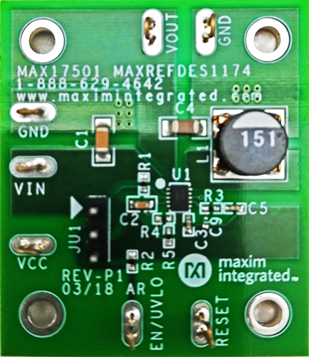

Overview
Design Resources
Design & Integration File
- Schematic
- PCB Layout
- BOM
- Test Results
- Tools & Models
Description
The MAXREFDES1181 is centered around the MAX17501 ultra small, high-efficiency, high-voltage, synchronous stepdown DC-DC converter with integrated MOSFETs. This design provides a -5V output and up to 150mA of load current with an input voltage range of 18V to 30V. Unlike a traditional design, this reference design is configured to work in an inverting buck-boost topology to produce negative output voltage from positive input voltage.
Industrial control equipment such as programmable logic controllers, I/O modules, mass flow controllers, and various other sensors and supporting systems use analog components like amplifiers and multiplexers that operate on negative supply voltage. The MAXREFDES1181 is designed to demonstrate the operation and principles on how to use the MAX17501 to provide a negative supply voltage.
Features & Benefits
Parts Used
Details Section
The MAXREFDES1181 is centered around the MAX17501 ultra small, high-efficiency, high-voltage, synchronous stepdown DC-DC converter with integrated MOSFETs. This design provides a -5V output and up to 150mA of load current with an input voltage range of 18V to 30V. Unlike a traditional design, this reference design is configured to work in an inverting buck-boost topology to produce negative output voltage from positive input voltage.
Industrial control equipment such as programmable logic controllers, I/O modules, mass flow controllers, and various other sensors and supporting systems use analog components like amplifiers and multiplexers that operate on negative supply voltage. The MAXREFDES1181 is designed to demonstrate the operation and principles on how to use the MAX17501 to provide a negative supply voltage.
Other features include the following:
- No Schottky-Synchronous Operation for High Efficiency and Reduced Cost
- Ultra-Compact Layout
- All-Ceramic Capacitors
- Reduces Power Dissipation
This reference design is a single negative output power supply using the MAX17501 synchronous step-down DC-DC converter. The power supply is designed for applications that require operation at negative supply voltage. This design can deliver up to 150mA at -5V. Table 1 shows an overview of the design specification.
| PARAMETER | SYMBOL | MIN | MAX |
| Input Voltage | VIN | 18V | 30V |
| Output Voltage | VOUT | -5V | |
| Output Current | IOUT | 0mA | 150mA |
| Efficiency | η | 86% | |
| Switching Frequency | fSW | 600kHz | |
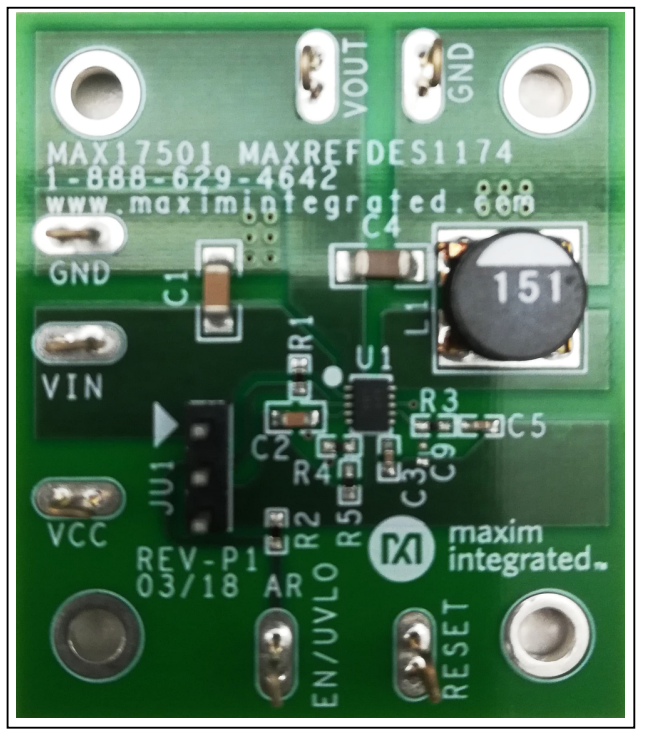
This document describes the MAXREFDES1181 variant on the MAXREFDES1174 hardware shown in Figure 1. It provides a detailed, systematic technical guide for the design of the MAXREFDES1181 using the MAX17501 synchronous step-down DC-DC converter for applications that require negative supply voltage. See the MAX17501 data sheet for device operation details. The power supply has been built and tested, details of which follow later in this document.
Because the MAX17501 is used in a buck-boost configuration for this design, the formula used is for a buck-boost converter instead of the traditional buck converter formula provided in the MAX17501 data sheet. Before starting the design process, we need to determine the appropriate version for the MAX17501, the operating input voltage range, the duty ratio, and the load current capability of our design.
Part Number Selection
The MAX17501 is available in six different versions. The MAX17501A/MAX17501E and MAX17501B/MAX17501F have preset output voltages of 3.3V and 5.0V, respectively. An internal compensation network is used to produce the preset output. Because of the internal compensation, these versions cannot be used to produce the negative output voltage.
The MAX17501G/MAX17501H offer an adjustable output voltage from 0.9V to 92% VIN that can be set with a resistive voltage-divider connected from the positive terminal of the output capacitor (VOUT) to GND. Because this design is used in a negative output configuration, ensure that only version G and version H are used in the design. The switching frequency is at 600kHz for the G version and 300kHz for the H version. The MAX17501GATB+ is used in this reference design.
Operating Input Voltage Range
The MAX17501 is rated for a 4.5V to 60V input voltage range. In negative output configuration, the input voltage seen by the part is the difference between input voltage and output voltage. Therefore, for negative output voltage, the maximum voltage input and the absolute value of the output voltage must not exceed 60V, as shown in the following equation:

At -5V output, the input voltage range is from 4.5V to 55V. The 18V to 30V input voltage range used in this design is within the specifications.
Duty Ratio
Assuming the ideal situation where the power losses associated with the MOSFETs and the inductor DC resistance can be ignored, the duty ratio is expressed as follows:

At 18V, 24V, and 30V voltage input, the duty ratio is at 0.22, 0.17, and 0.14, respectively. The maximum duty ratio is at the minimum input voltage. Therefore, the DMAX is at 0.22. Note that the formula used is for a buck-boost converter.
Load Current Capability
In inverting applications, the switch current is expected to be higher. Although this part is rated for 500mA output current, the maximum output current for this design will be less. With a maximum duty cycle of 22%, the maximum output current is given by the following equation:

The maximum output load is 390mA, which is sufficient for the 150mA output load used in this design.
Step 1: Inductor Selection
The MAXREFDES1181 utilizes continuous current mode, where the current through the inductor never drops to 0A. The inductor is exposed to current throughout the entire switching period. The rules of thumb for inductor selection are as follows:
- Inductance value (L): The value must be within the value range where it is high enough to prevent excessive current, but low enough so that sufficient energy can be stored in the inductor core for current conduction.
- Inductor saturation current (ISAT): The saturation current rating must be above the peak current limit value (0.76A is typical for the MAX17501) to ensure that the inductor can store the required energy without saturating.
- DC resistance (RDCR): The DC resistance value must be as low as possible to minimize the self-heating effect and to reduce losses.
The minimum value for the inductor is calculated using the following equation:

where ∆IL can be expressed in terms of the inductor current ripple ratio, LIR:
∆IL=LIRxIOUT(MAX)=0.5 500mA=250mA
and LIR is assumed to be 0.5.
The maximum value for the inductor is calculated by the following equation:

Taking into consideration the ISAT and RDCR, the inductor chosen was the LPS6235-333MR rated at 33µH. Because the inductor is chosen, the ∆IL value is calculated based on the actual value chosen for the application. This ∆IL should be used in the next design requirement and is given by the following equation:

Step 2: Input Capacitor Selection
The input capacitor is important to reduce the current peaks drawn from the input supply, increase efficiency, and reduce noise injection. The value of CIN largely depends on the source impedance of the input supply. The higher the source impedance is, the higher the input capacitance required. To reduce the voltage ripple at the input, a ceramic capacitor is placed right at the input of the MAX17501. For industrial standards, an X7R ceramic capacitor is recommended. The minimum value needed for this design is given by the following equation:

Considering the derating value of the capacitor, the GRM31MR71H474KA01 rated at 0.47µF/50V, 10%, X7R was chosen.
Step 3: Output Capacitor Selection
The output capacitance is important to ensure the stability of the system and is usually sized to support a step load of 50% of the maximum output current in the application, so the output-voltage deviation is contained to ±3% of the output-voltage change. A ceramic capacitor with very low ESR should be used. The minimum value required is calculated by the following equation:

Considering the derating value of the capacitor, the GRM31CR71H225KA88 rated at 2.2µF/50V, 10%, X7R was chosen.
Step 4: Output Voltage Settings
The output voltage can be set using the voltage-divider connected at the FB node. R4 is connected from VOUT to the FB node, while R5 is connected from FB to GND. For the MAX17501G, the parallel combination of R4 and R5, RP, must be less than 15kΩ. To optimize efficiency and output accuracy, use the following equations to choose the values of R4 and R5:

The standard resistor values chosen are 84.5kΩ and 18.7kΩ respectively. The parallel combination for R4 and R5 is calculated as follows:

The RP value is 15kΩ, which is within the specification.
Step 5: Turn-On Voltage Input Selection
The EN/UVLO is driven high to enable the output voltage. The input voltage (undervoltage threshold) at which the device turns on can be set with a resistive voltage-divider connected from VIN to GND. R1 is connected from VIN to the EN/UVLO node, and R2 is connected from the EN/UVLO node to GND. For adjustable output voltage devices, VINU must be higher than 0.8 × VOUT. Therefore, the VINU for this design must be higher than 4V. A 3.3MΩ value is chosen for R1. The R2 value is then given by the following equation:

where VINU is 18V. A standard resistor value of 261kΩ was used in this design.
Step 6: External Loop Compensation
The switching mode power supply (SMPS) requires a feedback control to regulate the output requirements when the input of the system changes. The loop compensation is required to ensure the stability of the overall loop response and to ensure that the output voltage is kept constant, regardless of changes in the input voltage or load current. A gain margin greater than 6dB and a 45-degree phase margin typically provide stability to the system. The compensation component values, R3 and C5, are calculated using the following equations:

where k = 2 for the MAX17501.

The standard values for R3 and C5 are 12.1kΩ and 3.9nF, respectively
Step 7: Soft-Start Capacitor Selection
To reduce inrush current, the MAX17501 implements an adjustable soft-start operation. A capacitor connected from the SS pin to GND programs the soft-start period. For this design, the soft-start period is set at 1.2ms. The soft-start capacitor value is calculated using the following equation:

A standard capacitor value of 6.8nF was used in this design.
Documentation & Resources
-
MAXREFDES1181 Design Files7/9/2019ZIP6 M
-
EE-Sim OASIS Free Simulator7/9/2019
Support & Training
Search our knowledge base for answers to your technical questions. Our dedicated team of Applications Engineers are also available to answer your technical questions.