
MAXREFDES1176


Overview
Design Resources
Design & Integration File
- Schematic
- PCB Layout
- Bill of Materials
- Test Results
Description
Power over Ethernet (PoE) is a technology that allows network cables to deliver power to a powered device (PD) through power-sourcing equipment (PSE) or midspan, and has many advantages over traditional methods of delivering power. PoE allows power and data to be combined, removing the need for altering the AC mains infrastructure and can be installed by non-electricians. PoE is an intelligent system designed with protection at the forefront, preventing overload, underpowering, and installation errors, while allowing simple scalability and reliability.
The MAX17690 eliminates the need for an optocoupler or auxiliary transformer winding and achieves ±5% output voltage regulation over line, load, and temperature variations. The MAX17690 implements an innovative algorithm to accurately determine the output voltage by sensing the reflected voltage across the primary winding during the flyback time interval. By sampling and regulating this reflected voltage when the secondary current is close to zero, the effects of secondary-side DC losses in the transformer winding, the PCB tracks, and the rectifying diode on output voltage regulation can be minimized.
The MAX17690 also compensates for the negative temperature coefficient of the rectifying diode.
Features & Benefits
- IEEE® 802.3af/at Compliance
- Thermally Enhanced, 3mm × 3mm, 10-Pin TDFN Package (MAX5969B)
- 30V to 60V Input Voltage Range
- Programmable Switching Frequency from 50kHz to 250kHz
- Programmable Input Enable/UVLO Feature
- Programmable Input Overvoltage Protection
- Adjustable Soft-Start
- 2A/4A Peak Source/Sink Gate Drive Capability
- Hiccup Mode Short-Circuit Protection
- Fast Cycle-by-Cycle Peak Current Limit
- Thermal Shutdown Protection
- Space-Saving, 16-Pin, 3mm x 3mm TQFN Package
- -40°C to +125°C Operating Temperature Range
Details Section
Power over Ethernet (PoE) is a technology that allows network cables to deliver power to a powered device (PD) through power-sourcing equipment (PSE) or midspan, and has many advantages over traditional methods of delivering power. PoE allows power and data to be combined, removing the need for altering the AC mains infrastructure and can be installed by non-electricians. PoE is an intelligent system designed with protection at the forefront, preventing overload, underpowering, and installation errors, while allowing simple scalability and reliability.
The MAX17690 eliminates the need for an optocoupler or auxiliary transformer winding and achieves ±5% output voltage regulation over line, load, and temperature variations. The MAX17690 implements an innovative algorithm to accurately determine the output voltage by sensing the reflected voltage across the primary winding during the flyback time interval. By sampling and regulating this reflected voltage when the secondary current is close to zero, the effects of secondary-side DC losses in the transformer winding, the PCB tracks, and the rectifying diode on output voltage regulation can be minimized.
The MAX17690 also compensates for the negative temperature coefficient of the rectifying diode.
Other features include the following:
- IEEE® 802.3af/at Compliance
- Thermally Enhanced, 3mm × 3mm, 10-Pin TDFN Package (MAX5969B)
- 30V to 60V Input Voltage Range
- Programmable Switching Frequency from 50kHz to 250kHz
- Programmable Input Enable/UVLO Feature
- Programmable Input Overvoltage Protection
- Adjustable Soft-Start
- 2A/4A Peak Source/Sink Gate Drive Capability
- Hiccup Mode Short-Circuit Protection
- Fast Cycle-by-Cycle Peak Current Limit
- Thermal Shutdown Protection
- Space-Saving, 16-Pin, 3mm x 3mm TQFN Package
- -40°C to +125°C Operating Temperature Range
This reference circuit consists of the MAX5969B PD controller and an isolated no-opto flyback DC-DC converter using the MAX17690 and MAX17606 to demonstrate a 5V DC output application. A 1GbE RJ45 magnetic jack is also included as well as two diode bridges for separating data and DC power provided by an endspan or midspan PoE system. The low-resistance, on-chip MOSFETs ensure high efficiency at full load and simplifies layout. The power supply delivers up to 1.4A at 5V. Table 1 shows an overview of the design specification.
| Parameter | Symbol | Min | Max |
| Input Voltage | VIN | 30V | 60V |
| Power Range | PIN | 6.49W | 12.95W |
| Undervoltage Lockout Voltage | VUVLO | 29.4V | |
| Frequency | fSW | 143.3kHz | |
| Peak Efficiency at Full Load | ηMAX | 90% | |
| Efficiency at Minimum Load | ηMIN | 61% | |
| Output Voltage | VOUT | 5V | |
| Output Voltage Ripple | ∆VO | 50mV | |
| Maximum Output Current | IOUT | 1.4A | |
| Maximum Output Power | POUT | 7W | |
This document describes the hardware shown in Figure 1. It provides a detailed technical guide to designing a complete interface for a PD to comply with the IEEE 802.3af/at standard in a PoE class 3 system and an isolated no-opto flyback DC-DC converter using the MAX17690 controller and MAX17606 secondary-side synchronous MOSFET driver. The power supply has been built and tested.
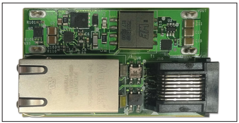
A PoE system delivers power and data to an end device (PD) typically through an RJ45 cable power from an endspan (PSE) (Figure 2) or a midspan (Figure 3). The power is separated from the data through diode bridges to deliver a typical 48V for efficient power transfer, which is low enough to be considered a safe voltage, and removes the need to rewire AC mains and saves cost.
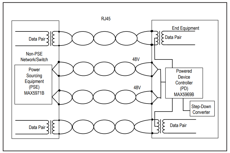
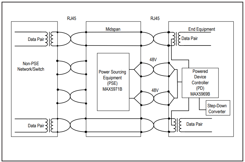
Although this voltage is safe for humans, it still can damage equipment if not properly delivered. This is where MAX5969B classification is required, ensuring the equipment can handle the power delivery. Before the PSE can enable power to a connected IP camera or other PD, it must perform a signature detection.
Signature Detection
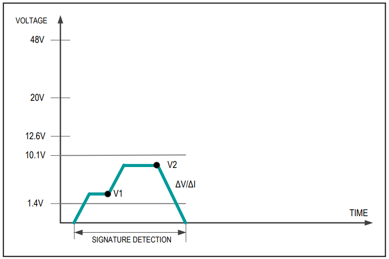
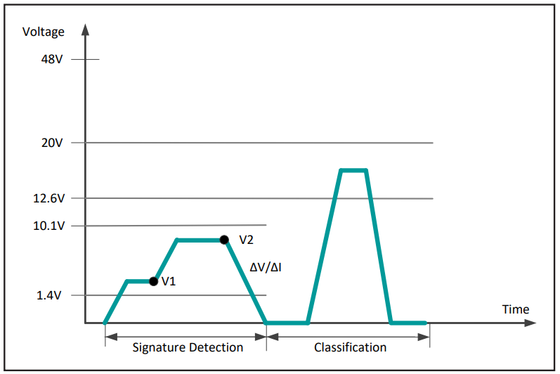
Signature detection uses a lower voltage to detect a characteristic signature of IEEE-compatible PDs (a 24.9kΩ resistance). See Figure 4. Once this signature has been detected, the PSE knows that higher voltages can be safely applied. The PSE applies two voltages on VIN in the range of 1.4V to 10.1V (1V step minimum) and then records the current measurements at the two applied voltages. The PSE then computes the change in current when each voltage was applied (ΔV/ΔI) to ensure the presence of the 24.9kΩ signature resistor.
Classification
In classification mode, the PSE classifies the PD based on the power consumption required. (The IEEE 802.3af/ at standard defines only class 0 to 4 and class 5 for any special requirement.)
An external resistor (RCLS) of 43.7Ω connected from CLS to VSS sets the classification current. The PSE determines the class of a PD by applying a voltage at the PD input and measuring the current sourced from the PSE.
When the PSE applies a voltage between 12.6V and 20V, the MAX5969A/MAX5969B exhibit a current of 26mA to 30mA. The PSE uses the classification current information to classify the power requirement of the PD (MAX5969B).
The classification current includes the current drawn by RCLS and the supply current of the MAX5969A/MAX5969B so the total current drawn by the PD is within the IEEE 802.3af/at standard figures. The classification current is turned off whenever the device is in power mode (Figure 5).
Power Mode
The final stage after detection and classification of a newly connected PD is to enable power. The 48V supply from the PSE is connected to the PD through the RJ45 cable. Once enabled, the PSE continues to monitor the amount of current being delivered to the PD and cuts power to the cable if the power drawn is not within the correct range. This protects the PSE against overload, underpowering and ensuring that the PSE is disconnected from the cable if the PD is unplugged or faulted. See Figure 6.
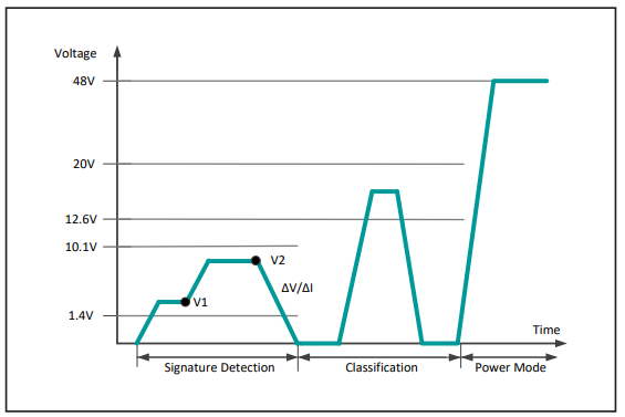
The MAX5969B enters power mode when VIN rises above the undervoltage lockout threshold (VON). Note that VON/VOFF = 38.6V/31V for the MAX5969B. When VIN rises above VON, the MAX5969B turns on the internal n-channel isolation MOSFET to connect GND to RTN. The open-drain power-good output (PG) remains low for a minimum of tDELAY until the power MOSFET fully turns on to keep the downstream DC-DC converter disabled during inrush. The PGOOD open-drain output is also connected to three small-signal transistors to prevent the DC converters from powering up before the power from the PD is allowable.
| Class | Maximum Power Used by PD (W) | RCLS (Ω) | VIN* (V) | Class Current Seen at VIN (mA) | IEEE 802.3af/at PSE Classification Current Specification (mA) | ||
| Min | Max | Min | Max | ||||
| 0 | 0.44 to 12.95 | 619 | 12.6 to 20 | 0 | 4 | 0 | 5 |
| 1 | 0.44 to 3.94 | 117 | 12.6 to 20 | 9 | 12 | 8 | 13 |
| 2 | 3.84 to 6.49 | 66.5 | 12.6 to 20 | 17 | 20 | 16 | 21 |
| 3 | 6.49 to 12.95 | 43.7 | 12.6 to 20 | 26 | 30 | 25 | 31 |
| 4 | 12.95 to 25.5 | 30.9 | 12.6 to 20 | 36 | 44 | 35 | 45 |
| 5 | > 25.5 | 21.3 | 12.6 to 20 | 52 | 64 | — | — |
*VIN is measured across the MAX5969A/MAX5969B input VDD to VSS.
Place the input capacitor, classification resistor, and transient voltage suppressor as close as possible to the MAX5969A/MAX5969B. Use large SMT component pads for power dissipating devices such as the MAX5969A/MAX5969B and the external diodes. Use short and wide traces for high-power paths.
The MAX5969B enters undervoltage lockout when the input voltage drops below 31V. When the input drops below this value, the isolation MOSFET switches off, disconnecting the 48V from the buck converters. The MAX5969B exits undervoltage lockout when the input exceeds 38.6V.
Design Procedure for No-Opto Flyback Converter Using MAX17690
The converter design process can be divided into three parts: the power stage design, the setup of the MAX17690 no-opto flyback controller, and closing the control loop. This document is intended to complement the information contained in the MAX17690 data sheet.
The following design parameters are used throughout this document:
| Symbol | Function |
| VIN | Input voltage |
| VUVLO | Undervoltage turn-on threshold |
| VOVI | Overvoltage turn-off threshold |
| tSS | Soft-start time |
| VOUT | Output voltage |
| ΔVO | Steady-state output ripple voltage |
| IOUT | Output current |
| POUT | Output power |
| η(MAX) | Target efficiency at maximum load |
| η(MIN) | Target efficiency at minimum load |
| PIN | Input power |
| fSW | Switching frequency |
| D | Duty cycle |
| nSP | Secondary-primary turns ratio |
Throughout the design procedure reference is made to the schematic. See the Design Resources section.
Part I: Designing the Power Components
Step 1: Calculate the Minimum Turns Ratio for the Flyback Transformer
The secondary-primary turns ratio, nSP, and the duty cycle, D, for the flyback converter are related by the flyback DC gain function as follows:

The converter’s absolute minimum input voltage is the undervoltage lockout threshold (VIN falling), which is programmed with a resistor-divider for the MAX17690. At this voltage and at maximum output power, D should be less than or equal to 66% (maximum duty cycle at which the MAX17690 can operate) to ensure reliable converter operation. For the current design, the undervoltage lockout threshold (VIN falling) occurs at 29V, so with D set at 66%, the absolute minimum turns ratio, nSP(MIN), for the flyback transformer is calculated as follows
nSP(MIN) = 0.10
This transformer turns ratio assumes that there are no DC voltage drops in the primary and/or secondary circuits. In practice, a larger transformer turns ratio must be chosen to account for these DC voltage drops. For the current design, a transformer turns ratio of nSP = 0.25 was chosen.
Step 2: Estimate the Maximum and Minimum Duty Cycle Under Normal Operating Conditions
Normal input voltage operating conditions are defined as VIN(MIN) and VIN(MAX) on page 1. By using the flyback DC gain function again, the duty cycle is estimated as:

nSP and VOUT are fixed so clearly DMAX occurs when VIN is a minimum, i.e., at VIN(MIN). For the current design, VIN(MIN) = 30V, so:
DMAX = 0.43
The MAX17690 derives the current, ΔILP, in the primary magnetizing inductance by measuring the voltage, ΔVRCS, across the current-sense resistor (RCS) during the on-time of the primary-side MOSFET. So:

ΔILP is a maximum at DMAX and VIN(MIN) and a minimum at DMIN and VIN(MAX), so:

and

Solving these two equations:

where ΔVRCS(MIN) and ΔVRCS(MAX) correspond to the minimum current limit threshold (20mV) and the maximum current limit threshold (100mV) of the MAX17690, respectively. So, for VIN(MIN) = 30V, VIN(MAX) = 60V, and DMAX = 0.43, we have:
DMIN = 0.057
Step 3: Calculate the Maximum Allowable Switching Frequency
The isolated no-opto flyback topology requires the primary side MOSFET to constantly maintain switching, otherwise there is no way to sense the reflected secondary-side voltage at the drain of the primary-side MOSFET. The MAX17690 achieves this by having a critical minimum on-time, tON(CRIT), for which it drives the MOSFET. At a given switching frequency tON(MIN) corresponds to DMIN. From the MAX17690 data sheet, the critical minimum on-time tON(CRIT) for the NDRV pin is 235ns. We can therefore calculate the maximum allowable switching frequency to ensure that tON(MIN) > tON(CRIT), as follows:

Because DMIN is fixed by ΔVRCS(MIN), ΔVRCS(MAX), DMAX, VIN(MIN), and VIN(MAX), then tON(MIN) can be chosen arbitrarily larger than tON(CRIT) so that fSW is less than fSW(MAX). With tON(MIN) = 398ns the switching frequency is as follows:

Note that the MAX17690 should always be operated in the 50kHz to 250kHz switching frequency range and tON(MIN) must be chosen accordingly to ensure that this constraint is met.
Step 4: Estimate the Primary Magnetizing Inductance
Maximum input power is given by:
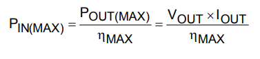
For the discontinuous flyback converter, all energy stored in the primary magnetizing inductance (LP) during the MOSFET on-time is transferred to the output during the MOSFET off-time, i.e., the full power transfer occurs during one switching cycle. Therefore, because E = P x t, we have:

The maximum input energy must be stored in LP during the on-time of the MOSFET, so:

We also know that the peak current in LP, ΔILP(MAX) occurs at input voltage VIN(MIN) and MOSFET on-time tON(MAX), so:

and substituting:
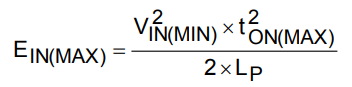
Combining with the original P x t equation gives:

Finally, by rearranging we have an expression for the primary magnetizing inductance LP:

Estimating the power converter efficiency at 90% and with VIN(MIN) = 30V, DMAX = 0.43, VOUT = 5V, and fSW = 143.34kHz, then:
LP(MAX) ≈ 55.9µH
This inductance represents the maximum primary magnetizing inductance, since it sets the current-limit threshold. Choosing a larger inductance sets the current-limit threshold at a lower value and could cause the converter to go into current limit at a value lower than IOUT, which would be undesirable. For the current design, we have chosen a primary inductance of 42μH ±10%:
LP ≈ 42μH ±10%
Step 5: Recalculate DMAX, DMIN, and tON(MIN) Based on the Selected Value for LP
Rearranging the LP equation in Step 4 gives an expression for DMAX as follows:

Referring to Step 2:

and:

Step 6: Calculate the Peak and RMS Currents in the Primary Winding of the Flyback Transformer
The peak primary winding current occurs at VIN(MIN) and DMAX according to the following equation:

The RMS primary winding current can be calculated from ΔILP(MAX) and DMAX as follows:

Step 7: Calculate the Peak and RMS Currents in the Secondary Winding of the Flyback Transformer
The peak current in the flyback transformer’s secondary-side winding can be established by considering that the entire energy transferred from the primary-side winding to the secondary-side winding is delivered to the load during one switching period. Again, because E = P x t:

Substituting:

And rearranging:

Current flows in the secondary-side winding of the flyback transformer while the secondary-side rectifying device is conducting. This conduction time, tON(SEC), is calculated using the inductor volt-second equation:

where V = VOUT, L = LS, dI = ΔILS(MAX), and dt = tON(SEC), so:

The maximum duty cycle of the secondary-side rectifying device, DS(MAX), can now be calculated:

Finally, the RMS secondary winding current can be calculated from ΔILS(MAX) and DS(MAX) as follows:

Step 8: Summarize the Flyback Transformer Specification
All the critical parameters for the flyback transformer have been calculated and are summarized below. Using these parameters, a suitable transformer can be designed.
| Parameter | Symbol | Value |
| Primary Magnetizing Inductance | LP | 42µH ±10% |
| Primary Peak Current | ΔILP(MAX) | 1.61A |
| Primary RMS Current | ILP(RMS) | 0.53A |
| Turns Ratio (NS/NP) | nSP | 0.25 |
| Secondary Peak Current | ∆ILS(MAX) | 6.1A |
| Secondary RMS Current | ILS(RMS) | 2.60A |
Step 9: Calculate Design Parameters for Secondary-Side Rectifying Device
Depending on the output voltage and current, a choice can be made for the secondary-side rectifying device. Generally, for output voltages above 12V at low currents (less than 1A), Schottky diodes are used, and for voltages less than 12V synchronous rectification (MOSFET) is used. The current design is a 5V/1.4A output converter, so we outline a procedure for selecting a suitable MOSFET for the synchronous switch.
Figure 7 shows a simplified schematic with the synchronous MOSFET, QS. The MAX17606 is a secondary-side synchronous driver and controller specifically designed for the isolated flyback topology operating in Discontinuous Conduction Mode (DCM) or Border Conduction Mode (BCM).
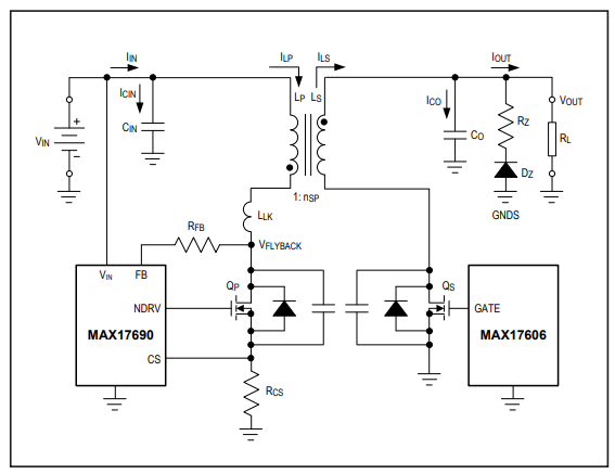
The important parameters to consider for the synchronous rectifying device are the same as those of a regular rectifying diode: peak instantaneous current, RMS current, voltage stress, and power losses. Because QS and LS are in series, they experience the same peak and RMS currents, so:
IQS(RMS) = ILS(RMS) = 2.60A
and
IQS(MAX) = ∆ILS(MAX) = 6.1A
When QS is off, VIN reflected to the secondary side of the flyback transformer plus (VOUT + VQS(SAT)) is applied across the drain-source of QS, so:
VQS(MAX) = nSP x VIN(MAX) + VOUT + VQS(SAT)
= 0.25 x 60V + 5V + (1.16A x 18mΩ)
≈ 20V
QS has both conduction losses due to its RDS(ON) and switching losses. Allowing for reasonable design margin, we chose the Infineon® BSZ040N04LSG for this design with the following specifications:
| Parameter | Value |
| Maximum Drain-Source Voltage | 40V |
| Continuous Drain Current | 40A |
| Drain-Source Resistance | 6.1mΩ |
| Minimum VGS Threshold VGSTH | 1.2V |
| Typical VGS Plateau VGSPL | 3.0V |
| Maximum QG(T) | 64nC |
| Typical QGD | 4.9nC |
| Total Output Capacitance COSS | 1100pF |
The power losses in the QS can be approximated as follows:
PTOT = PCON + PCDS + PSW ≈ 82mW
where:
PCON is the loss due to IQS(RMS) flowing through the drain-source on resistance of QS:
PCON = I2QS(RMS) x RDS(ON) ≈ 41mW
PCDS is the loss due to the energy in the drain-source output capacitance being dissipated in QS at turn-on:

and PSW is the turn-on voltage-current transition loss that occurs as the drain-source voltage decreases and the drain current increases during the turn-on transition:

where IDRV is the maximum drive current capability of the MAX17606’s GATE output and IQS(t-ON) is the instantaneous current in QS at turn-on. IQS(t-ON) is equal to IQS(MAX).
Step 10: Calculate Design Parameters for Primary-Side MOSFET
The important parameters to consider for the primary-side MOSFET (QP) are peak instantaneous current, RMS current, voltage stress, and power losses. Because QP and LP are in series they experience the same peak and RMS currents, so from Step 6:
IQP(MAX) = ΔILP(MAX) ≈ 1.61A
and
IQP(RMS) = ILP(RMS) ≈ 0.53A
When QP turns off, VOUT reflected to the primary side of the flyback transformer plus VIN(MAX) is applied across the drain source of QP. In addition, until QS starts to conduct, there is no path for the leakage inductance energy to flow through. This causes the drain-source voltage of QP to rise even further. The factor of 1.5 in the equation below represents this additional voltage rise; however, this factor can be higher or lower depending on the transformer and PCB leakage inductances:

Allowing for reasonable design margin, we chose the Fairchild FDMS86252 was chosen for this design with the following specifications:
| Parameter | Value |
| Maximum Drain-Source Voltage | 150V |
| Continuous Drain Current | 16A |
| Drain-Source Resistance | 98mΩ |
| Minimum VGS Threshold VGSTH | 2V |
| Typical VGS Plateau VGSPL | 4V |
| Maximum QG(T) | 15nC |
| Typical QGD | 2.4nC |
| Total Output Capacitance COSS | 115pF |
The power losses in the QP can be approximated as follows:
PTOT = PCON + PCDS + PSW ≈ 96mW
where:
PCON is the loss due to IQP(RMS) flowing through the drain-source on resistance of QP:
PCON = I2QP(RMS) x RDS(ON) ≈ 27mW
PCDS is the loss due to the energy in the drain-source output capacitance being dissipated in QP at turn-on:

And PSW is the turn-on voltage-current transition loss that occurs as the drain-source voltage decreases and the drain current increases during the turn-on transition:

where IDRV is the maximum drive current capability of the MAX17690’s NDRV output and IQP(t-ON) is the instantaneous current in QP at turn-on. Because the flyback converter is operating in DCM, IQP(t-ON) is zero and so is PSW.
Step 11: Select the RCD Snubber Components
Referring to Figure 8, when QP turns off, ILP charges the output capacitance, COSS, of QP. When the voltage across COSS exceeds the input voltage plus the reflected secondary to primary voltage, the secondary-side diode (or synchronous switch) turns on. Because the diode (or synchronous switch) is now on, the energy stored in the primary magnetizing inductance is transferred to the secondary; however, the energy stored in the leakage inductance continues to charge COSS since there is nowhere else for it to go. Because the voltage across COSS is the same as the voltage across QP, if the energy stored in the leakage inductance charges COSS to a voltage level greater than the maximum allowable drain-source voltage of QP, the MOSFET fails.

One way to avoid this situation arising is to add a suitable RCD snubber across the transformer’s primary winding. In Figure 8, the snubber is labeled RSN, CSN, and DSN. In this situation, when QP turns off, the voltage at Node A is:
VNODEA = VCSN + VIN
When the secondary-side diode (or synchronous switch) turns on, the voltage at Node B is:

So, the voltage across the leakage inductance is:

So:

The average power dissipated in the snubber network is:

Substituting ΔtSN into this expression we have:

The leakage inductance energy is dissipated in RSN, so from:

We can calculate the required RSN as follows:

Over one switching cycle we must have:

So, we can calculate the required CSSN as follows:

Generally, ΔVCSN should be kept to approximately 10% to 30% of VCSN. Figure 9 illustrates VCSN, ΔISN, and ΔtSN. The voltage across the snubber capacitor, VCSN, should be selected so that:
VCSN < VDSMAX(QP) – VIN(MAX)
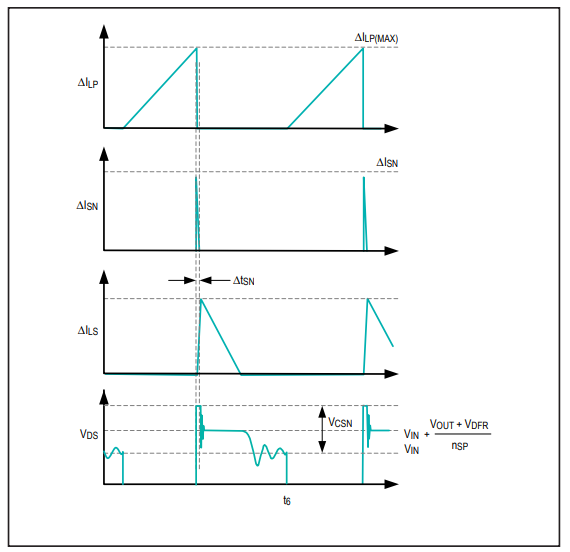
Choosing too large a value for VCSN causes the voltage on the QP drain to get too close to its maximum allowable drain-source voltage, while choosing too small a value results in higher power losses in the snubber resistor. A reasonable value should result in a maximum drain voltage on QP that is approximately 75% of its maximum allowable value. The worst-case condition for the snubber circuit occurs at maximum output power when:
ΔISN = ΔILP(MAX)
Assuming the leakage inductance is 1.5% of the primary inductance, choosing VCSN = 54V and ΔVCSN = 5.4V, we get the following approximate values:
PSN = 188mW
RSN = 15.5kΩ
CSN = 4.7nF
Finally, we consider the snubber diode, DSN. This diode should have at least the same voltage rating as the MOSFET, QP. Although the average forward current is very low, it must have a peak repetitive current rating greater than ΔILP(MAX).
Step 12: Calculate the Required Current-Sense Resistor
From Step 4 we have the maximum input power given by:

For the DCM flyback converter all the energy stored in the primary magnetizing inductance, LP, during the MOSFET on-time is transferred to the output during the MOSFET off-time, i.e., the full power transfer occurs during one switching cycle. Therefore, since E = P x t, we have:
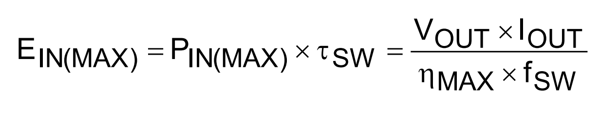
The maximum input energy must be stored in LP during the primary-side MOSFET on-time, so:

Substituting the equations above:

and
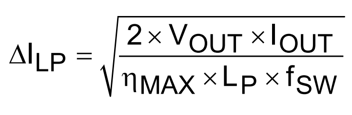
From Step 2 we have:
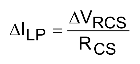
so:

A standard 60mΩ resistor was chosen for RCS.
Step 13: Calculate and Select the Input Capacitors
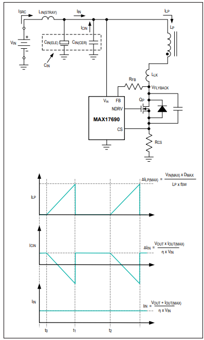
Figure 10 shows a simplified schematic of the primary side of the flyback converter and the associated current waveforms. In steady-state operation, the converter draws a pulsed high-frequency current from the input capacitor, CIN. This current leads to a high-frequency ripple voltage across the capacitor according to the following expression:
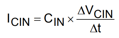
It is the ripple voltage arising from the amp second product through the input capacitor.
During the QP on-time interval from t0 to t1, the capacitor is supplying current to the primary inductance LP of the flyback transformer and its voltage is decreasing. During the QP off-time time interval from t1 to t2, no current is flowing in LP, and current is being supplied to capacitor from the input voltage source. According to the charge balance law, the decrease in capacitor voltage during time t0 to t1 must equal the increase in capacitor voltage during time t1 to t2. So:

And finally, since:

we have:

For maximum high-frequency ripple voltage requirement ΔVCIN, we can now calculate the required minimum CIN.
There is high-frequency AC current flowing in CIN, as shown in the center waveform of Figure 10. The selected capacitor must be specified to tolerate the maximum RMS current, ICIN(RMS). From the simplified schematic:
ILP = IIN + ICIN
Therefore:

where:
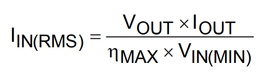
and from Step 6:

So:

An additional high-frequency ripple voltage is present due to this RMS current flowing through the ESR of the capacitor. Ceramic capacitors are generally used for limiting high-frequency ripple due to their high AC current capability and low ESR.
In addition to using a ceramic capacitor for high-frequency input ripple-voltage control as described above, an electrolytic capacitor is sometimes inserted at the input of a flyback converter to limit the input voltage deviation when there is a rapid output load change. A 100% load change gives rise to an input current transient of:

During this transient, there is a voltage drop across any series stray inductance, LIN(STRAY), that exists between the input voltage source and the input capacitor of the power supply. So from:

we have:

We now have two values for CIN. One for input high-frequency ripple-voltage control:

and a second for transient input voltage control:
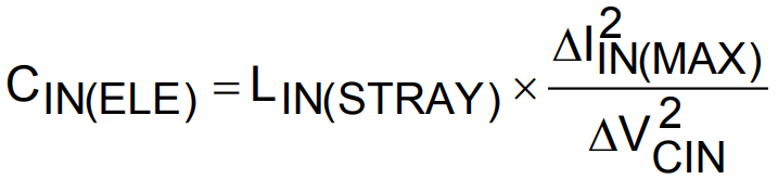
If CIN(ELE) > CIN(CER), both ceramic and electrolytic capacitors must be used at the input of the power supply and ΔVCIN should be limited to approximately 75mV to keep the AC current in the ESR of the electrolytic capacitor within acceptable limits. Otherwise, CIN(ELE) is not required. In this case, the value of CIN(CER) can be significantly reduced since there is no longer any requirement to limit ΔVCIN to less than 75mV. Based on the current design specification with LIN(STRAY) approximated at 50nH, we have:
CIN(CER) = 16.3µF
and
CIN(ELE) = 0.7µF
Since CIN(ELE) < CIN(CER), an electrolytic capacitor is not required. We can now recalculate CIN(CER) based on a ΔVCIN = 600mV:
CIN(CER) ≈ 2µF
Allowing for a ±10% capacitor tolerance and a further reduction of capacitance of 75% due to the DC bias effect (operating an 80V ceramic capacitor at 50V), our final nominal value of input capacitance required is:

This is achieved by using two 4.7µF ceramic capacitor (Murata GRM32ER71K475KE14). The AC current in the capacitor is:
CCIN(RMS) ≈ 0.46ARMS
which is well within specification for the selected capacitor.
Step 14: Calculate and Select the Output Capacitor
High-frequency ripple voltage requirements are also used to determine the value of the output capacitor in a flyback converter.
Figure 11 shows a simplified schematic of the secondary side of the flyback converter and the associated current waveforms.
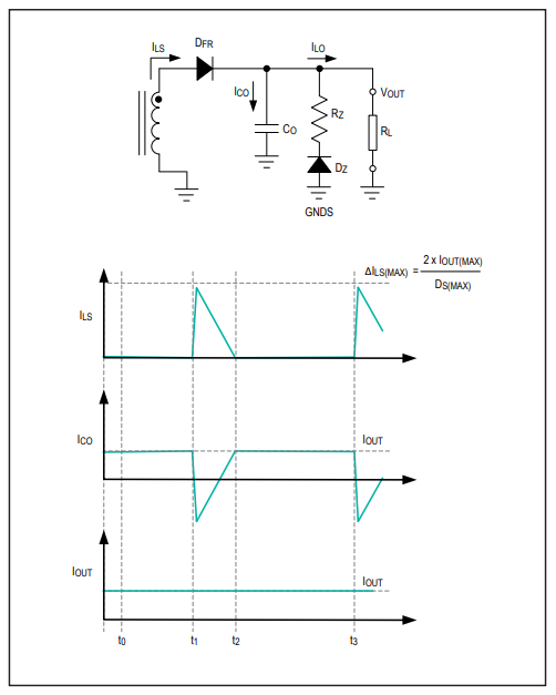
In steady-state operation, the load draws a DC current from the secondary side of the flyback converter. By examining the secondary current waveforms, we see that CO is supplying the full output current IOUT to the load during the time interval from t2 to t3. During this time interval, the voltage across CO decreases. At time t3, QP has just turned off and the secondary rectifying diode DFR (or the secondary synchronous switch QS) starts to conduct supplying current to the load and to CO. The charging and discharging of CO leads to a high-frequency ripple voltage at the output according to the following expression:

Again, as with the input capacitor, this is the ripple voltage arising from the amp second product through the output capacitor.
By the capacitor charge balance law, the decrease in capacitor voltage during time t2 to t3 must equal the increase in capacitor voltage during time t1 to t2. When the capacitor is discharging, we have:

Finally, since:

We have:
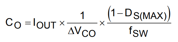
For maximum high-frequency ripple voltage requirement ΔVCO, we can now calculate the required minimum CO.
CO ≈ 102.2µF
As with the input capacitor, an additional high-frequency ripple voltage occurs at the output due to the output capacitor’s ESR and can be minimized by choosing a capacitor with low ESR. Also, as with the input capacitor, there is high-frequency AC current flowing in CO, as shown in the center waveform of Figure 11. The selected capacitor must be specified to tolerate this maximum RMS current, ICO(RMS). From the simplified schematic:
ILS = IOUT + ICO
Therefore:

where:
IOUT(RMS) = IOUT
and from Step 7:

so:

| Power Component | QTY | Description |
| Flyback Transformer | 1 | PRI. INDUCTANCE = 42µH SEC-PRI TURNS RATIO = 0.25 PEAK. PRI CURRENT = 1.61A PRI. RMS CURRENT = 0.53A PEAK SEC. CURRENT = 6.1A SEC. RMS CURRENT = 2.60A SWITCHING FREQ. = 143.3kHz |
| Input Capacitor | 2 | CAPACITOR; SMT (1210); CERAMIC CHIP 4.7µF; 80V; 10%; X7R Murata GRM32ER71K475KE14 |
| Output Capacitors | 3 | CAPACITOR; SMT (1210); CERAMIC CHIP 100µF; 6.3V; 20%; X7R Murata GRM32ER60J107ME20 |
| Primary MOSFET | 1 | MOSFET; NCH; I-(16A);
V-(150V) Fairchild FDMS86252 |
| Synchronous MOSFET | 1 | MOSFET; NCH; I-(40A);
V-(40V) Infineon BSZ040N04LSG |
If we allow for a ±20% capacitor tolerance and a further reduction of capacitance of 57% due to the DC bias effect (operating a 6.3V ceramic capacitor at 5V), our final nominal value is:

We can achieve this by placing three 100µF ceramic capacitors (Murata GRM32ER60J107ME20) in parallel. The minimum output capacitance using the above combination is 103.2µF. The AC current in each capacitor is:

which is well within specification for the selected capacitor.
Step 15: Summarize the Power Component Design
A first pass at calculating the power components in the no-opto flyback converter using MAX17690 has been completed. Referring to the schematic, a summary of the power components is listed below:
Part II: Setting Up the MAX17690 No-Opto Flyback Controller
Step 16: Setting Up the Switching Frequency
The MAX17690 can operate at switching frequencies between 50kHz and 250kHz (subject to the considerations in Step 3). A lower switching frequency optimizes the design for efficiency, whereas increasing the switching frequency allows for smaller inductive and capacitive components sizes and costs. A switching frequency of 143.3kHz was chosen in Step 3. R9 sets the switching frequency according to the following expression:

where R9 is in kΩ and fSW is in Hz.
Step 17: Setting Up the Soft-Start Time
The capacitor C6 connected between the SS pin and SGND programs the soft-start time. A precision internal 5μA current source charges the soft-start capacitor C6. During the softstart time, the voltage at the SS pin is used as a reference for the internal error amplifier during startup. The soft-start feature reduces inrush current during startup. Since the reference voltage for the internal error amplifier is ramping up linearly, so too is the output voltage during soft-start. The soft-start capacitor is chosen based on the required soft-start time (10ms) as follows:
C6 = 5 x tSS ≈ 50nF
where C6 is in nF and tSS is in ms. A standard 47nF capacitor was chosen.
Step 18: Setting Up the UVLO and OVI Resistors
A resistor-divider network of R1, R3, and R2 from VIN to SGND sets the input undervoltage lockout threshold and the output overvoltage inhibit threshold. The MAX17690 does not commence its startup operation until the voltage on the EN/ UVLO pin (R3/R2 node) exceeds 1.215V (typ). When the voltage on the OVI pin (R1/R3 node) exceeds 1.215V (typ), the MAX17690 stops switching, thus inhibiting the output. Both pins have hysteresis built in to avoid unstable turn-on/turnoff at the UVLO/EN and OVI thresholds. After the device is enabled, if the voltage on the UVLO/EN pin drops below 1.1V (typ), the controller turns off; after the device is OVI inhibited, it turns back on when the voltage at the OVI pin drops below 1.1V (typ). Whenever the controller turns on, it goes through the soft-start sequence. For the current design R1 = 10kΩ, R2 = 487kΩ, and R3 = 11kΩ give rise to an UVLO/EN threshold of 29.4V and an OVI threshold of 61.7V.
Step 19: Placing Decoupling Capacitors on VIN and INTVCC Pins
As previously discussed, the MAX17690 no-opto flyback controller compares the voltage VFLYBACK to VIN. This voltage difference is converted to a proportional current that flows in R5. The voltage across R5 is sampled and compared to an internal reference by the error amplifier. The output of the error amplifier is used to regulate the output voltage. The VIN pin should be directly connected to the input voltage supply. For robust and accurate operation, a ceramic capacitor (C2 = 1µF) should be placed between VIN and SGND as close as possible to the IC.
VIN powers the MAX17690’s internal low dropout regulator. The LDO’s regulated output is connected to the INTVCC pin. A ceramic capacitor (C3 = 2.2µF min) should be connected between the INTVCC and PGND pins for the stable operation over the full temperature range. Place this capacitor as close as possible to the IC.
Step 20: Setting Up the Feedback Components
RSET (R5), RFB (R4, R18), RRIN (R8), RVCM (R6), and RTC (R7) are critically important to achieving optimum output voltage regulation across all specified line, load and temperature ranges.
RSET resistor (R5): This resistor value is optimized based on the IC’s internal voltage to current amplifier and should not be changed.
RFB resistor (R4, R18): The feedback resistor is calculated according to the following equation:

Since we are using a synchronous MOSFET for rectification on the secondary side, we can assume that δVDFR/ δT = 0, so:

From the MAX17690 data sheet, VSET = 1V. The two resistors R4 = 182kΩ and R18 = 20kΩ form RFB. Using one high value resistor and one low value resistor in series allows slight adjustment to the series resistance combination so that the output voltage can be fine-tuned to its required value, if necessary.
RIN resistor (R8): The internal temperature compensation circuitry requires a current proportional to VIN. RRIN establishes this current and is calculated according to the following equation:
RRIN ≈ 0.6 x RFB
RVCM resistor (R6): The MAX17690 generates an internal voltage proportional to the on-time volt-second product. This enables the device to determine the correct sampling instant for VFLYBACK during the QP off-time. Resistor R6 is used to scale this internal voltage to an acceptable internal voltage limit in the device. To calculate the resistor, we must first calculate a scaling constant as follows:

After KC is calculated, the R6 value can be selected from the table below by choosing the resistance value that corresponds to the next largest KC.
| KC | R6 |
| 640 | 0Ω |
| 320 | 75kΩ |
| 160 | 121kΩ |
| 80 | 220Ω |
| 40 | Open |
In the present case, R6 = 121kΩ.
RTC resistor (R7): The value of RTC can then be calculated using the previous expression, restated below:

Since we are using a synchronous MOSFET for secondary-side rectification, we can assume that the temperature coefficient δVDFR/δT is zero so RTC should be infinite (i.e., open circuit).
This completes the setup of the MAX17690 no-opto flyback controller.
Part III: Closing the Control Loop
Step 21: Determine the Required Bandwidth
The bandwidth of the control loop determines how quickly the converter can respond to changes at its input and output. If we have a step change in output current, the voltage across the output capacitor decreases as shown in Figure 12.
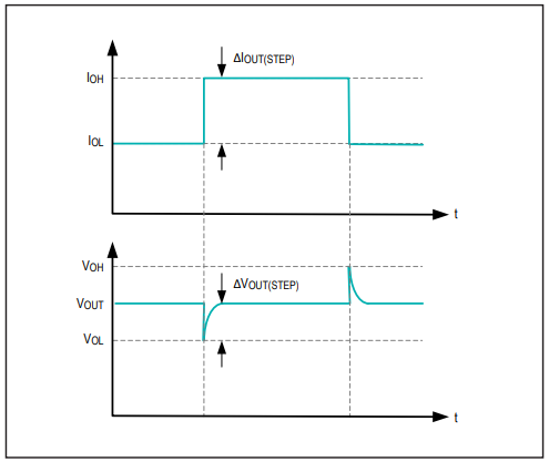
The control loop detects this reduction in output voltage and increases the duty cycle of QP to supply more current to the output capacitor. The amount of time required by the control loop to increase the duty cycle from its minimum value to its maximum value is the response time, τRES, of the control loop. For the MAX17690 we have:
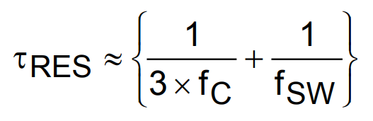
where fC is the bandwidth of the power converter. If we apply a switching load step of amplitude ΔISTEP, at a frequency of (1/τRES) and a 50% duty cycle then, to limit the output voltage deviation to ±ΔVOUT(STEP) we must have a minimum output capacitance of:

Combining the two previous equations, we have:

It is normal to specify ΔVOUT(STEP) for a load step from 50% to 100% of the maximum output current. We have already calculated CO(MIN) = 102.2µF in Step 14, fSW = 143.3kHz, so based on a 3% maximum ΔVOUT(STEP):
fC ≈ 8.9KHz
Step 22: Calculate the Loop Compensation
The MAX17690 uses peak current-mode control and an internal transconductance error amplifier to compensate the control loop. The control loop is modeled, as shown in Figure 13, by a power modulator transfer function GMOD(S) an output-voltage feedback transfer function GFB(S) and an error amplifier transfer function GEA(S).
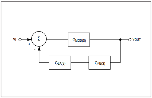
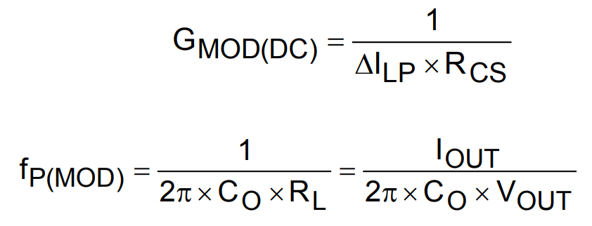
The power modulator has a pole located at fP(MOD) determined by the impedance of the output capacitor CO and the load impedance RL. It also has a zero at fZ(MOD) determined by the impedance of CO and the ESR of CO. The DC gain of the power modulator is determined by the peak primary current ΔILP and the current-sense resistor RCS. So:
and:
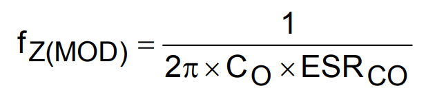
The output voltage feedback transfer function GFB(S) is independent of frequency and has a DC gain determined by VIN, VFLYBACK, and VSET as follows:

The MAX17690’s transconductance error amplifier should be set up in a configuration to compensate for the pole at fP(MOD) and the zero at fZ(MOD) of the modulator. This can be achieved by a Type II transconductance error amplifier compensation shown in Figure 14.
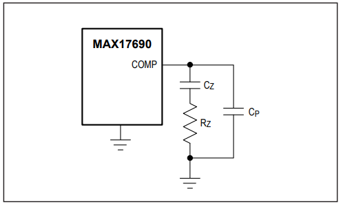
This compensation scheme type has a low frequency pole at fP-LF(EA) due to the very large output resistance RO (30MΩ to 50MΩ) of the operational transconductance amplifier (OTA). It has a zero at fZ(EA) determined by CZ and RZ of the compensation network, and it has an additional pole at fP(EA) determined by CP and RZ of the compensation network. So:

and:

To achieve stable operation, we must ensure that:
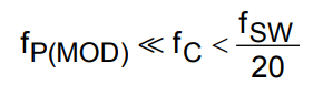
Set the closed-loop gain at fC equal to 1:
GMOD(fC) × GFB(fC) × GEA(fC) = 1
Place the zero in the error amplifier network at the same frequency as the pole in the power modulator transfer function:

The frequency fZ(MOD) at which the zero occurs in the power modulator transfer function depends on the ESR of CO. If ceramic capacitors are used for CO, fZ(MOD) will be generally much higher than fC. However, if the ESR of CO is large, fZ(MOD) could be lower than fC. This is a very important point since both the gain of the power modulator at fC, and the gain of the error amplifier at fC depend on whether fZ(MOD) is greater than or less than fC. This is illustrated in Figure 15.
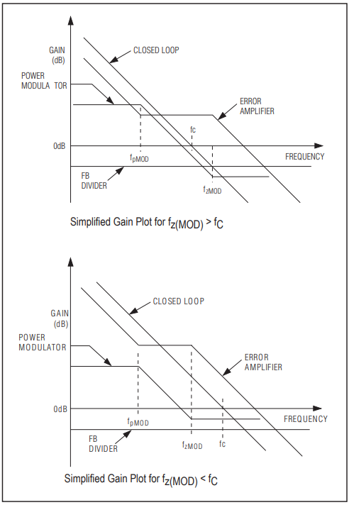
By examining the gain plots in Figure 15, we see that for fZ(MOD) > fC:

and for fZ(MOD) < fC:
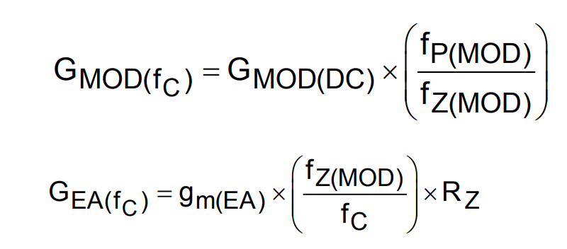
For the current design, we have:

and:

Since fZ(MOD) > fC:

and since GFB is independent of frequency, we have:

We can now set the closed-loop gain equal to 1 as follows:

Rearranging we can calculate:

Substituting ΔILP from Step 12:

Finally, we can calculate the remaining components, CZ and CP, in the error amplifier compensation network as follows:

and:

Documentation & Resources
-
MAXREFDES1176 Design FIles3/3/2021ZIP3 M
Support & Training
Search our knowledge base for answers to your technical questions. Our dedicated team of Applications Engineers are also available to answer your technical questions.