


Overview
Design Resources
Design & Integration File
- Schematic
- PCB Layout
- Firmware
- Bill of Materials
- Test Results
Description
The MAXREFDES1152 is a four-channel universal analog input that measures voltage or current signals. Each channel can be configured for voltage input at 0 to 10V or current input at 0 to 20mA. A 24V power supply can be switched out to power an external 2-Wire, 3-Wire, or 4-Wire sensor.
The MAXREFDES1152 provides a complete system solution for industry voltage and current measurement. The analog front end includes Beyond-the-Rails™ analog switches, and operational amplifiers are used to achieve voltage/ current input selection and signal conditions. The 24-bit MAX11270 analog-to-digital converter (ADC) is the heart of the system and achieves highly accurate measurements. The microcontroller communicates with the MAX11270 and the MAX7317 10-port I/O expander to control the analog front end and accept the ADC conversion results. The 24V field input power supply is isolated with the analog front end and with the microcontroller, which is powered by a USB power supply. This isolated design enhances system robustness in harsh industry applications.
The MAXREFDES1152 also integrates five Beyond-the- Rails single-pole/double throw (SPDT) analog switches (MAX14763); a dual Beyond-the-Rails 4:1 analog multiplexer (MAX14778); two ultraprecise, low-noise op amps (MAX44251); 2.75kVRMS data isolation (MAX14930 and MAX14932); an STMicroelectronics® STM32F1 microcontroller; a μp supervisory circuit (MAX6730); an FTDI Chip® USB-UART bridge; a high-efficiency iso-buck DC-DC converter (MAX17681); and isolated/regulated +5V and +3.3V power rails (two MAX16910s) and -5V power rail (MAX1697). The entire system typically operates at less than 500mW and fits into a 5cm × 10.6cm space. While targeted for industrial and PLC applications, the MAXREFDES1152 can be used in any application that requires high-accuracy analog-to-digital conversion.
Features & Benefits
- Highly accurate measurements
- 0 to +10V voltage inputs
- 0 to 20mA current inputs
- Four channels
- Each channel can be configured for voltage or current input
- 24V input protection
- Isolated power and data
- Board calibration
- Connector provides 24V output
- 24V output can enable or disable
Parts Used
Details Section
The MAXREFDES1152 is a four-channel universal analog input that measures voltage or current signals. Each channel can be configured for voltage input at 0 to 10V or current input at 0 to 20mA. A 24V power supply can be switched out to power an external 2-Wire, 3-Wire, or 4-Wire sensor.
The MAXREFDES1152 provides a complete system solution for industry voltage and current measurement. The analog front end includes Beyond-the-Rails™ analog switches, and operational amplifiers are used to achieve voltage/ current input selection and signal conditions. The 24-bit MAX11270 analog-to-digital converter (ADC) is the heart of the system and achieves highly accurate measurements. The microcontroller communicates with the MAX11270 and the MAX7317 10-port I/O expander to control the analog front end and accept the ADC conversion results. The 24V field input power supply is isolated with the analog front end and with the microcontroller, which is powered by a USB power supply. This isolated design enhances system robustness in harsh industry applications.
The MAXREFDES1152 also integrates five Beyond-theRails single-pole/double throw (SPDT) analog switches (MAX14763); a dual Beyond-the-Rails 4:1 analog multiplexer (MAX14778); two ultraprecise, low-noise op amps (MAX44251); 2.75kVRMS data isolation (MAX14930 and MAX14932); an STMicroelectronics® STM32F1 microcontroller; a µp supervisory circuit (MAX6730); an FTDI Chip® USB-UART bridge; a high-efficiency iso-buck DC-DC converter (MAX17681); and isolated/regulated +5V and +3.3V power rails (two MAX16910s) and -5V power rail (MAX1697). The entire system typically operates at less than 500mW and fits into a 5cm × 10.6cm space. While targeted for industrial and PLC applications, the MAXREFDES1152 can be used in any application that requires high-accuracy analog-to-digital conversion.
Other features include:
- Highly accurate measurements
- 0 to +10V voltage inputs
- 0 to 20mA current inputs
- Four channels
- Each channel can be configured for voltage or current input
- 24V input protection
- Isolated power and data
- Board calibration
- Connector provides 24V output
- 24V output can enable or disable
The MAXREFDES1152 features four channels of analog input and supports voltage or current input signals with isolated power and data. The MAXREFDES1152 includes the following primary components: power supply, analog front end, ADC, and microcontroller.
The power supply generates all of the power rails used in the analog front end and ADC. The power is isolated with 24V input. The analog front end transfers the input signal to meet the ADC input range. A high-precision 24-bit ADC converts the analog input to digital signals that are read by the microcontroller. The microcontroller is isolated with the analog front end with digital isolator. Table 1 shows an overview of the hardware specification.
| Parameter | Symbol | Min | Max |
| Power supply | VCC | 20V | 36V |
| Supply current | ICC | 20mA | 25mA |
| Voltage Input | VIN | 0 | 15V |
| Current Input | IIN | 0 | 20mA |
| Input Current Clamp | ICLAMP | 22mA | 27mA |
| 24V Output Current | 24VO | 1.25A | Note: Power supply input current increase with power supply voltage increase due to on board protection. Maximum 24V output current depends on the input 24V power supply, but not larger than 1.25A. The reference design targets a voltage input range of 0-10V, but it can handle inputs of up to 15V. Maxim does not guarantee the accuracy of measurements taken with voltage inputs that are out of the design’s target range. |
This document describes the hardware and firmware. It provides a detailed system design, especially how the analog front end is achieved. This reference design has been built and tested, details of which follow later in this document.
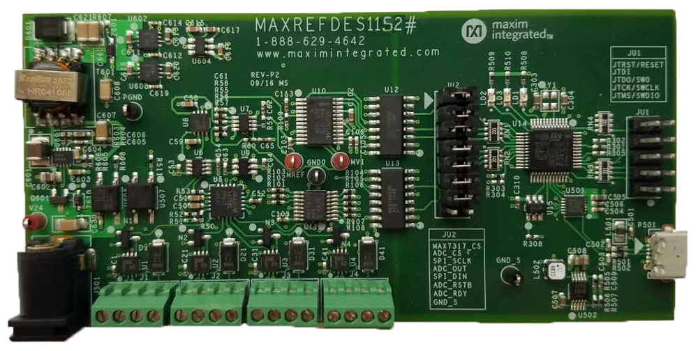
Note: MAXREFDES1152 replaces MAXREFDES146.
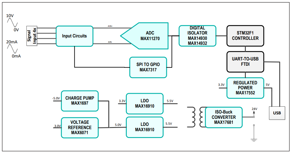
This section discusses the design components of the MAXREFDES1152. Figure 1 is an image of the hardware, which replaces the MAXREFDES146. Figure 2 is a block diagram of the system.
Analog Front-End Design
An analog switch is required for selecting the input, which can be configured for current or for voltage. When the input is configured for current, a sense resistor is used to convert the input from current to voltage. When the input is configured for voltage, high input impedance (commonly >100kΩ) is required. Because the input voltage can be up to 10V, the power supply voltage of the analog switch should be larger than 10V. For general switches, if the input voltage is 10V, then the power supply also must be 10V. In these cases, the design should include a power supply of 10V or larger to power the switch. The MAXREFDES1152, however, uses Beyond-the-Rails switches, which can support inputs of -25V to +25V with only 5V of power supply. The other 10V power supply is not necessary, which can reduce design complexity.
The Input section is the same for all four channels. The channels are connected to the MAX14778, which selects the input type. For voltage inputs, the four inputs use one voltage divider, simplifying calibration by requiring calibration on only one channel and applying the calibration results to all other channels. For current input, however, each channel has its own sense resistor, so for highly accurate measurements, calibration on each channel is required.
For more details about the analog front end, refer to Detailed Description of Hardware section.
ADC and Reference Selection
To meet highly accurate measurement requirements, select the MAX11270 24-bit 130dB SNR sigma delta ADC. In bypass mode, the MAX11270 can achieve 16.9 bits of noise-free resolution at a 1ksps data rate. For a voltage reference of 3V, the noise-free resolution is as follows:
(3V/2^16.9) × 2 = 49μV (bipolar mode)
For current input of 20mA, the sense resistor is 100Ω, so 1μA of current generates 100μV of voltage. A noise-free resolution of 49μV can ensure accurate measurements as low as 1μA.
The MAX11270 is a single-channel ADC that measures four channels of input. The ADC requires a switch on each channel for measurements, and it must work in singlecycle conversion mode. The maximum sample rate for single-cycle conversion mode is 1.6ksps. An additional delay time is required for switching from one channel to another and waiting for input voltage stability at the ADC input.
An input voltage of 10V or an input current of 20mA is conditioned to 2V and is fed into the ADC input. For some applications, however, a certain margin is required to detect the fault condition. Here, select the MAX6071A 3V voltage reference as the ADC reference. The MAX6071 is a highly accurate voltage reference with an initial accuracy of 0.04% and a maximum temperature coefficient (tempco) of 6ppm/°C.
Power Supply Design
The system is powered by a 24V field power supply. Field power supplies are commonly used in applications deployed in harsh environments, with significant noise that can negatively impact the accuracy of measurements. The analog section requires a very stable power supply to ensure highly accurate measurements. So, the design incorporates the MAX17681 iso-buck DC-DC converter, which generates an isolated 5.5V power supply; two MAX16910 low-cost LDOs to generate power supplies of +5V and +3.3V for the analog switches, operational amplifiers, reference, and ADC to ensure that the operational amplifier can work properly at zero input. A negative power supply is also required—the charge pump MAX1697 is used to generate a -5V rail for the operational amplifier. This also can help upgrade the input voltage range from 0–10V to -10V–+10V by changing several resistors in the analog front end without modifying the design.
Protection Design
The Diodes Incorporated® MMBT3904 and Zener diode form a voltage regulator that can prevent high-voltage transient pulses of up to 65V at the power supply input from causing damage to the device. The MAX14763 integrated ±2500V HMB ESD and ±750V CDM ESD, 24V TVS on each input channel can increase the protection and clamp the input to approximately 24V when the input is larger than 24V.
Overcurrent protection is achieved by using the Infineon® BSS159N. On current inputs, this protection is required to avoid damage when the input current is too large; on high-voltage inputs, overcurrent is required for when the channel is incorrectly configured for current input. In the event of overcurrent, the current generates a voltage through the sense resistor to limit the input current. For more details about the connection see the reference design schematic.
Digital Isolation Design
The microcontroller configures the ADC or reads the ADC conversion result through the serial peripheral interface (SPI). The channel selection setting and on-board 24V power supply switch is controlled by digital signals. To save the digital isolator, select the MAX7317 SPI-to-GPIO expander. The MAX7317 can expand to up to ten GPIO ports and is controlled by an SPI. The MAX7317 and MAX11270 ADC share the same SPI to reduce isolation channels. Only one MAX14930B and one MAX14932B are required to achieve the digital isolation for the microcontroller and analog sections.
The MAX14930B/MAX14932B is a four-channel, 2.75kVRMS digital isolator. It supports a data rate of up to 25Mbps. A low propagation delay allows the device to support high-speed SPI communication isolation.
Microcontroller Design
The on-board microcontroller is used to evaluate the performance of the universal analog input. The MAX17552 DC-DC converter generates the 3.3V power supply to power the microcontroller. The MAX17552 input is from the USB port. The MAX6730A watchdog monitor device monitors the microcontroller to ensure it works properly. It has an open-drain output, a long initial watchdog time-out period (35s min), and a short time-out period (1.12s) after the first valid WDI transition. The long initial watchdog time-out provides enough time to initialize the system after power-up.
The purpose of this reference design is to demonstrate the front-end performance and accuracy of ADC measurements. Because the reference design is meant only for testing in the lab, it does not use the MAX6730A watchdog monitor. In real-world industrial applications, however, the watchdog is required.
If customers want to provide their own firmware to control the system, they can remove the jumpers on JU2 and connect the external SPI and GPIO to JU2. This allows them to easily evaluate the universal analog input with different microcontrollers or their own firmware.
24V and GND On-Board Power Supply Switch
For the 4mA-to-20mA current transmitter sensor, the on-board 24V voltage can switch out to a power sensor. The 24V and GND switch are PhotoMOS® from Panasonic®. The 24V power supply GND and signal input GND are isolated when the GND switch is open. The 24V switch and GND switch can be controlled individually.
The 2-Wire and 3-Wire sensors must close the 24V and GND switch. The 4-Wire sensor must close the 24V switch and leave GND switch open. The sensor connection is listed in Figure 3.
The MAXREFDES1152 reference design has four channels of analog input with isolated power and data. It supports voltage and current inputs as shown in the configuration diagram in Figure 3. Each input circuitry utilizes digitally controlled analog switches (MAX14763) to make the appropriate electrical connections for different types of input signals.
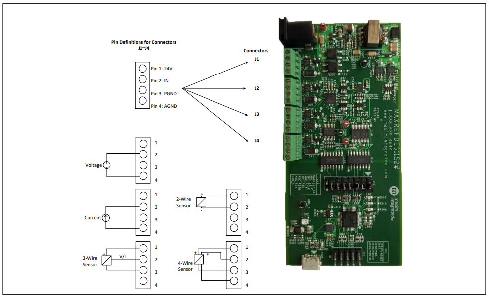
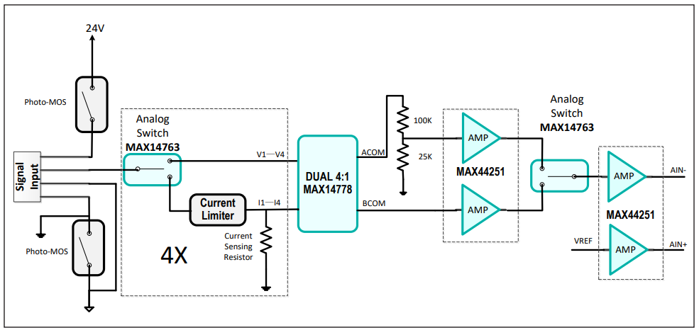
Figure 4 shows the analog front end, which converts the input voltage or current to an acceptable range for the ADC.
Voltage Input
The input is configured for voltages when the MAX14763 SEL is set LOW. Input voltage is routed to the MAX14778 to select the channel to be measured. A voltage divider (4:1) divides the MAX14778 ACOM output voltage. The MAX44251 ultraprecision amplifier buffers the divider voltage, as the MAX44251’s input bias current is 200pA and the offset is 7µV, so the high-resistance voltage divider does not decrease the accuracy. The buffered voltage is routed to another MAX14763—which selects whether to measure voltage or current to the ADC. The MAX14763 output voltage (VCOM) is fed into a unit gain differential amplifier. The output of differential amplifier is
VREF - VCOM
The ADC input voltage is the differential voltage of VREF and VREF - VCOM; that is,
VREF - (VREF - VCOM) = VCOM
Because VCOM is 1/5 of the input voltage, the input voltage is 5 × VCOM. As all four voltage input channels share the same voltage divider, only one channel needs to be calibrated—its results then apply to all other channels. This greatly simplifies the calibration process.
Current Input
The input is configured for current when the MAX14763 SEL is set HIGH. Input current flows through the sense resistor to generate a voltage, VI = I × RSENSE. Each current input channel has overcurrent protection, which limits the input current to approximately 22mA if the input current is larger than 22mA. Overcurrent protection helps to ensure the integrity of the internal circuit when the input current is too large or when there is high voltage because the input has been configured incorrectly as current. Input voltage VI is routed to the MAX14778 and switches to BCOM output. The BCOM output voltage is buffered with the MAX44251 and through the MAX14763 to a differential amplifier. The differential amplifier output is
VREF - VI
The ADC input voltage is the differential voltage of VREF and VREF - VI; that is,
VREF - (VREF - VI) = VI
As VI is I × RSENSE, the RSENSE value is a known resistor, then
I = VI/RSENSE
The ADC measures the VI, and the input current value can be calculated. Each channel has an RSENSE, so a current input calibration should be performed on each channel. Select a 0.1% accuracy RSENSE resistor and low temperature drift for better performance.
Control and Measurement
Control and measurement of the input current and voltage for each channel selection uses logic-level control.
All the control signals are from the MAX7317 SPI-to-GPIO expander. The MAX7317 and MAX11270 ADC share the same SPI.
The MAX11270 ADC is 24-bit sigma-delta ADC with low power and high SNR that can measure input accurately. The ADC’s reference input is driven by a high-precision voltage reference, the MAX6071A, with 0.04% initial accuracy and a 6ppm/°C maximum tempco. ADC conversion results can be read out through an SPI interface, which is isolated with the STM32F103 microcontroller by using the MAX14930 and MAX14932 four-channel 2.75KVRMS digital isolators. The on-board STM32 microcontroller controls all operations. Customers can provide their own SPI by removing shut on JU2 and connecting their own SPI to the system. This can help them evaluate the analog front-end performance with their own firmware.
Power
The analog front end is powered by an external 24V input power supply. The iso-buck MAX17681 generates an isolated 5.5V power supply. Two MAX16910 LDOs generate +5V and +3.3V rails from a +5.5V power supply. MAX1697 charge pump generates a -5V power rail from +5V input.
The system incorporates two on-board PhotoMOSes to support 2-Wire, 3-Wire, and 4-Wire sensors. One PhotoMOS can switch on/off the 24V input voltage to the connector in order to power the external sensor. The other PhotoMOS can switch on/off the 24V input power supply GND and analog front-end GND.
The MAX17552 step-down DC-DC converter converts the +5V supply from the USB to +3.3V and powers the STM32 microcontroller and FTDI USB-UART bridge. Three LEDs can be used as indicators for system operation.
The MAXREFDES1152 uses the on-board STM32F1 microcontroller to control the analog switch and communicate with the ADC. The user reads the sampled data through a terminal program, allowing analysis on any third-party software. The user can also perform system calibrations through a terminal program. The simple process flow is shown in Figure 5. The firmware is written in C using the IAR tool.
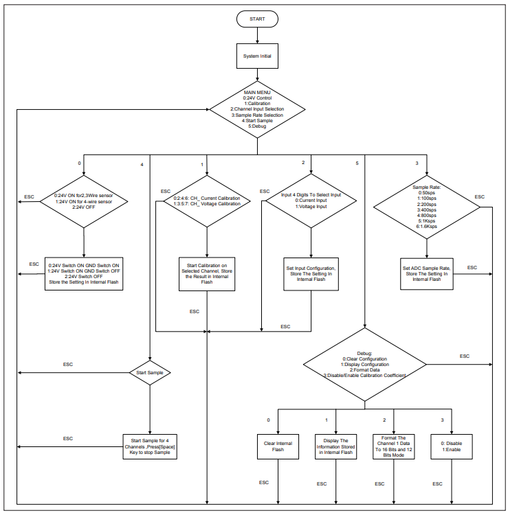
The firmware accepts the channel set, calibration, sampling and debug commands, communication with the PC through a standard terminal program by way of a virtual COM port. The complete source code is provided to facilitate customer development. Code documentation can be found in the corresponding firmware platform files.
Documentation & Resources
-
MAXREFDES1152 Design Files7/9/2019ZIP11 M
-
MAXREFDES1152: Four-Channel Universal Analog Input Using the MAX112707/9/2019PDF738 K
Support & Training
Search our knowledge base for answers to your technical questions. Our dedicated team of Applications Engineers are also available to answer your technical questions.