

Overview
Design Resources
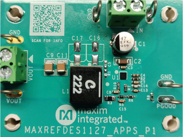
Description
The MAXREFDES1127 demonstrates how to build a DC-DC buck converter using the MAX18066 for 2.5V DC output applications from a 10.8V to 13.2V input. This reference design delivers up to 3A at 2.5V output. This design uses a two-layer board.
The MAX18066 current-mode, synchronous, DC-DC buck converters deliver an output current up to 4A with high efficiency. The devices operate from an input voltage of 4.5V to 16V and provide an adjustable output voltage from 0.606V to 90% of the input voltage. The devices are ideal for distributed power systems, notebook computers, non-portable consumer.
The devices feature a pulse-width modulation (PWM) mode operation with an internally fixed switching frequency of 500kHz capable of 90% maximum duty cycle. The devices automatically enter skip mode at light loads. The current-mode control architecture simplifies compensation design and ensures a cycle-by-cycle current limit and fast response to line and load transients. Additional features include an externally adjustable soft-start, independent enable input and power-good output for power sequencing, and thermal shutdown protection. The devices offer overcurrent protection (high side sourcing) with hiccup mode during an output short-circuit condition. The devices ensure safe startup when powering into a pre-biased output.
Parts Used
Details Section
The MAXREFDES1127 demonstrates how to build a DC-DC buck converter using the MAX18066 for 2.5V DC output applications from a 10.8V to 13.2V input. This reference design delivers up to 3A at 2.5V output. This design uses a two-layer board.
The MAX18066 current-mode, synchronous, DC-DC buck converters deliver an output current up to 4A with high efficiency. The devices operate from an input voltage of 4.5V to 16V and provide an adjustable output voltage from 0.606V to 90% of the input voltage. The devices are ideal for distributed power systems, notebook computers, non-portable consumer.
The devices feature a pulse-width modulation (PWM) mode operation with an internally fixed switching frequency of 500kHz capable of 90% maximum duty cycle. The devices automatically enter skip mode at light loads. The current-mode control architecture simplifies compensation design and ensures a cycle-by-cycle current limit and fast response to line and load transients. Additional features include an externally adjustable soft-start, independent enable input and power-good output for power sequencing, and thermal shutdown protection. The devices offer overcurrent protection (high side sourcing) with hiccup mode during an output short-circuit condition. The devices ensure safe startup when powering into a pre-biased output.
A small size, high-efficiency, synchronous step-down converter using the MAX18066 is shown for a 2.5V/3A application. Table 1 provides an overview of the design specification. The measured data and waveforms from the hardware set up can be found in the Test results.
| PARAMETER | SYMBOL | MIN | TYP | MAX |
| Input Voltage | VIN | 10.8V | 12V | 13.2V |
| Frequency | fSW | 500kHz | ||
| Efficiency | η | >85% | ||
| Output Voltage | VOUT | 2.5V | ||
| Load Step | ISTEP | 2A to 3A | ||
| Transient Deviation | ΔVOUT | 75mV | ||
| Output Voltage Ripple | VPK-PK | 25mV | ||
| Output Current | IOUT | 0A | — | 3A |
| Output Power | POUT | 7.5W | ||
This document describes the hardware shown in Figure 1. It provides a detailed, systematic technical guide for the design of a buck converter using the MAX18066 for high voltage and smaller size. For the device operation details, refer to the MAX18066 data sheet and the MAX18066 EV kit data sheet. The power supply has been built and tested, details of which follow later in this document.
Required Equipment
- AC-DC Power Supply: Chroma Systems 62015L-60-6
- Electronic Load: Keithley® 2380-120-60
- Oscilloscope: Teledyne® LeCroy® WaveSurfer® 3024z
- Multimeter: Keithley DMM6500
Procedure
The reference design is fully assembled and tested. Follow these steps to verify board operation:
- Connect the positive and negative terminals of the power supply to the input connector.
- Set the power-supply voltage to 12V and the current limit to 3A.
- Turn on the power supply.
- Verify that VOUT is close to 2.5V using the digital multimeter (DMM).
- Verify that the switching frequency is close to 500kHz by monitoring the switching node voltage with the oscilloscope.
Design Procedure for a High-Efficiency Buck Converter
For this reference design, the design process is divided into the following stages:
- Output-Voltage Selection
- Inductor Selection
- Input Capacitor Selection
- Output Capacitor Selection
- Compensation Network
- BIAS Capacitor Selection
- Soft Start Capacitor Selection
- PCB Layout Guidelines
This document complements the information contained in the MAX18066 data sheet.
The following design parameters are used throughout this document:
| SYMBOL | FUNCTION |
| VIN | Input voltage |
| VOUT | Output voltage |
| IOUT | Output current |
| fSW | Switching frequency |
| D | Duty cycle |
| ΔIL(P-P) | Peak to Peak Inductor Ripple Current |
Step 1: Output-Voltage Selection
Set the output voltage using the R5 and R6 resistors. VFB is the internal reference voltage, and its minimum value is 0.6V.
Setting VOUT = 2.5V and VFB = 0.6V gives
R5 = R6 x 3.1667
select R6 = 10kΩ, which gives R5 = 31.6kΩ.
Step 2: Inductor Selection
Inductor is selected based on LIR. LIR is the ratio of the peak-to-peak inductor current ripple to the average value of the inductor current. We have chosen an inductor value to produce a current ripple (ΔIL) equal to 50% of load current, giving a LIR of 0.5.
Inductance value required to meet the current ripple:
Off the shelf inductor of 2.2μH is chosen.
Additionally, we must ensure that the following relationships are satisfied:
and
and
Where,
ILSAT - Rated Saturation Current of the Inductor
ILRMS - Rated RMS Current of the Inductor
IPEAK - Peak Current through the Inductor
ILRMS - RMS Current through the Inductor
Hence:
We choose the Coilcraft® XAL1060-222ME with 2.2µH inductance and 20A ILSAT and 24A ILRMS saturation current.
Step 3: Input Capacitor Selection
The input capacitor RMS current requirement (IRMS) is defined by the following equation:
where IOUT(MAX) is the maximum load current. IRMS has a maximum value when the input voltage equals twice the output voltage (VIN = 2 × VOUT), so IRMS = IOUT(MAX)/2. Required RMS current rating of the input capacitor is 1.5A.
The following equation shows the capacitor requirement for a target voltage ripple at the input:
IOUT is the maximum output current in amps and fSW is the switching frequency. Input capacitor is designed for an Input voltage ripple (ΔVQ) of 1%. Here CIN = 12.86µF. Due to the capacitor's DC bias characteristic and temperature characteristics, some margin should be reserved. We have used a combination of ceramic and electrolytic capacitors to meet both the capacitance and RMS current requirement. Hence, we have chosen Electrolytic capacitance = 47µF and Ceramic capacitance = (10µF || 0.1µF) for this design.
Step 4: Output Capacitor Selection
Use the following equations to calculate the output capacitance value due to load transient:
∆ILOAD is the load step current in amps and fCO is the unity gain bandwidth (or zero-crossing frequency). Output capacitor is designed for an output voltage overshoot of 3% for 1A load change and zero-crossing frequency of 50kHz. Here COUT is calculated as 88.88µF. Due to the capacitor’s DC bias characteristic and temperature characteristics, some margin should be reserved. Hence ceramic capacitors of capacitance = 2×47µF is used in this design.
For the capacitance chosen the output voltage ripple due to ESR and capacitance are calculated as:
ΔVESR is calculated as 3mV and ΔVQ is calculated as 4.82mV. So, the total output voltage ripple comes as 7.82mV which is within the specified limit of 25mV.
Step 5: Compensation Network
The IC uses the current mode-control scheme for a buck controller. A series resistor (R7) and a capacitor (C13) is required to have a stable, high-bandwidth loop in applications where ceramic capacitors are used for output filtering. For other types of capacitors, due to the higher capacitance and ESR, the frequency of the zero created by the capacitance and ESR is lower than the desired closed-loop crossover frequency. To stabilize a non-ceramic output-capacitor loop, add another compensation capacitor (C14) from COMP to GND to cancel this zero.
We chose R7 = 5.11kΩ, C13 = 8.2nF and C14 = 120pF. An additional RC circuit was added across the top feedback resistor to boost the phase margin. A R5 = 31.6kΩ and C15 = 820pF are selected.
Step 6: Bias Capacitor Selection
The internal circuitry of the IC requires a 5V bias supply. An internal 5V linear regulator generated this supply. The VDD pin is bypassed with a 1µF ceramic capacitor (C4) to guarantee stability under full-load condition.
Step 7: Soft Start Capacitor Selection
The devices utilize a soft start feature to ramp up the regulated output voltage slowly to reduce input inrush current during startup. Connect a capacitor of 0.1uF (C7) from SS to GND to set the startup time to 12ms.
Step 8: PCB Layout Guidelines
Careful PCB layout is critical to achieve low switching power losses and clean, stable operation. Use a multilayer board whenever possible for better noise immunity.
Follow the guidelines below for a good PCB layout:
- All connections carrying pulsed currents must be very short and as wide as possible. The inductance of these connections must be kept to an absolute minimum due to the high di/dt of the currents. If the loop area is made very small, then the inductance reduces because the inductance of a current-carrying loop is proportional to the area enclosed by the loop. Additionally, small current loop areas reduce radiated EMI.
- A ceramic input filter capacitor should be placed close to the IC’s VIN pins. Also, its ground loop to GND should be short. This eliminates as much trace inductance effects as possible and gives the IC a cleaner voltage supply. A bias capacitor for the VDD pin should also be placed close to the pin to reduce the effects of trace impedance. Its ground loop to GND should be short.
- When routing circuitry around the IC, the analog small-signal ground and power ground for switching currents must be kept separate. They should be connected where switching activity is minimal, typically the return terminal of the VDD bias capacitor. Doing so helps keep the analog ground quiet. The ground plane should be kept continuous and unbroken as far as possible. No trace-carrying, high-switching current should be placed directly over any ground plane discontinuity.
- PCB layout also affects the thermal performance of the design. A few thermal vias that connect to a large ground plane should be provided under the IC’s exposed pad for efficient heat dissipation. The PCB size, copper thickness, and board layer numbers affect the temperature dissipation capacity of the board. For this reference design, it can support a 3A load current with 2oz of copper, two layers, and 61mm x 46mm board.
Documentation & Resources
-
MAXREFDES1127 Design Files11/21/2021ZIP1 M
-
MAXREFDES1127: 2.5V/3A, Synchronous Step-Down Converter Using the MAX1806611/21/2021PDF464 K
Support & Training
Search our knowledge base for answers to your technical questions. Our dedicated team of Applications Engineers are also available to answer your technical questions.