

Overview
Design Resources
Design & Integration File
- Schematic
- Bill of Materials
- PCB Layout
- Test Results
Description
The MAX15038 is a synchronous buck converter which delivers up to 4A load current at output voltages from 0.6V to 90% of VIN. The integrated circuit (IC) supports the input voltage from 2.9V to 5.5V. The total output error is less than ±1% overload, line, and temperature ranges. The MAX15038 features fixed-frequency pulse-width modulation (PWM) mode operation with a switching frequency range of 500kHz to 2MHz set by an external resistor. It also provides the option of operating in a skip mode to improve light-load efficiency. High-frequency operation allows for small-size external components and an all-ceramic capacitor design. The low-resistance integrated nMOS switches ensure high efficiency at heavy loads while minimizing critical inductances, making the layout a much simpler task with respect to discrete solutions.
The MAX15038 comes with a high-bandwidth (28MHz) voltage-error amplifier. The voltage-mode control architecture and the voltage-error amplifier permit a Type III compensation scheme to be utilized to achieve maximum loop bandwidth, up to 20% of the switching frequency. High loop bandwidth provides fast transient response, resulting in less required output capacitance and allowing for all-ceramic capacitor designs.
The MAX15038 provides two three-state logic inputs to select one of the nine preset output voltages. The preset output voltages allow users to achieve ±1% output-voltage accuracy without using expensive 0.1% resistors. In addition, the output voltage can be set to any custom value by either using two external resistors at the feedback with a 0.6V internal reference or applying an external reference voltage to the reference input (REFIN). The MAX15038 offers programmable soft-start time using one capacitor to reduce input inrush current.
Features & Benefits
- Internal 31mΩ RDS(ON) high-side and 24mΩ RDS(ON) low-side metal-oxide semiconductor field-effect transistors (MOSFETs)
- Continuous 4A output current over temperature
- ±1% output accuracy overload, line, and temperature
- Soft-start reduces inrush supply current
- 500kHz to 2MHz adjustable switching frequency
- Monotonic startup for safe-start into prebiased outputs
- Selectable forced PWM or skip mode for light-load efficiency
- Overcurrent and overtemperature protection
- Output current sink/source capable with cycle-by- cycle protection
- Open-drain power-good output
Parts Used
Details Section
The MAX15038 is a synchronous buck converter which delivers up to 4A load current at output voltages from 0.6V to 90% of VIN. The integrated circuit (IC) supports the input voltage from 2.9V to 5.5V. The total output error is less than ±1% overload, line, and temperature ranges. The MAX15038 features fixed-frequency pulse-width modulation (PWM) mode operation with a switching frequency range of 500kHz to 2MHz set by an external resistor. It also provides the option of operating in a skip mode to improve light-load efficiency. High-frequency operation allows for small-size external components and an all-ceramic capacitor design. The low-resistance integrated nMOS switches ensure high efficiency at heavy loads while minimizing critical inductances, making the layout a much simpler task with respect to discrete solutions.
The MAX15038 comes with a high-bandwidth (28MHz) voltage-error amplifier. The voltage-mode control architecture and the voltage-error amplifier permit a Type III compensation scheme to be utilized to achieve maximum loop bandwidth, up to 20% of the switching frequency. High loop bandwidth provides fast transient response, resulting in less required output capacitance and allowing for all-ceramic capacitor designs.
The MAX15038 provides two three-state logic inputs to select one of the nine preset output voltages. The preset output voltages allow users to achieve ±1% output-voltage accuracy without using expensive 0.1% resistors. In addition, the output voltage can be set to any custom value by either using two external resistors at the feedback with a 0.6V internal reference or applying an external reference voltage to the reference input (REFIN). The MAX15038 offers programmable soft-start time using one capacitor to reduce input inrush current.
- Internal 31mΩ RDS(ON) high-side and 24mΩ RDS(ON) low-side metal-oxide semiconductor field-effect transistors (MOSFETs)
- Continuous 4A output current over temperature
- ±1% output accuracy overload, line, and temperature
- Soft-start reduces inrush supply current
- 500kHz to 2MHz adjustable switching frequency
- Monotonic startup for safe-start into prebiased outputs
- Selectable forced PWM or skip mode for light-load efficiency
- Overcurrent and overtemperature protection
- Output current sink/source capable with cycle-by-cycle protection
- Open-drain power-good output
In this document, a synchronous step-down DC-DC converter using the MAX15038 is demonstrated for a 3.3V output application. The power supply delivers up to a maximum load current of 4A. Table 1 shows an overview of the design specifications.
| PARAMETER | SYMBOL | MIN | TYP | MAX |
| Input Voltage | VIN | 4.5V | 5V | 5.5V |
| Frequency | fS | 800kHz | ||
| Efficiency | η | > 90% | ||
| Output Voltage | VOUT | 3.3V | ||
| Output Voltage Ripple | ΔVOUT | < 33mV | ||
| Maximum output current | IOUT(MAX) | 4A | ||
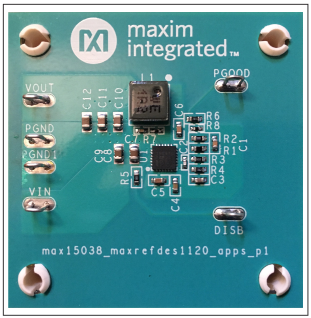
This document describes the hardware shown in Figure 1. It provides a detailed systematic technical guide to designing a step-down (buck) converter using the MAX15038. The power supply has been built and tested, details of which follow later in this document.
Switching regulators are very prominent in the industry today. The main advantage of using switching regulators instead of linear regulators is that they are far more efficient. They can achieve efficiencies of over 90%, whereas linear regulators have a typical 40% efficiency rating.
One of the most popular switching regulator topologies is the DC-DC step−down converter, also known as the buck converter. Buck converters are used to step a voltage down from a higher level to a lower level. There are two types of buck converters —synchronous and asynchronous.
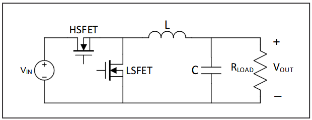
The synchronous buck converter is shown in Figure 2, which comprises two power MOSFETs, an inductor, and an output capacitor. The MOSFET that connects the input and the inductor is called a high-side MOSFET (HSFET). The MOSFET that connects the inductor and ground is called a low-side MOSFET (LSFET). In this topology, the switching of HSFET and LSFET are actively controlled by two complimentary control signals to prevent the MOSFETs from turning on simultaneously.
The asynchronous buck converter replaces the LSFET by a diode. This not only simplifies the control scheme, but also reduces the efficiency of the buck as there are more power losses on the diode.
This reference design discusses how asynchronous buck converter like the MAX15038 uses this type of topology. The detailed operation of the synchronous buck converter is described in the following sections.
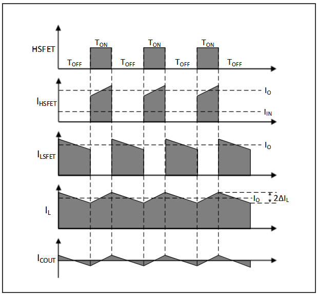
When HSFET is on and LSFET is off, current is supplied to the load through the HSFET. The voltage that appears across the inductor is VIN – VOUT. During this time, the energy is stored in the inductor. The current through the inductor increases with the rate of (VIN – VOUT)/L.
When HSFET is off and LSFET is on, the voltage across the inductor is now in reverse polarity -VOUT. The energy that had been stored in the inductor is released. The current through the inductor decreases with the rate of -VOUT/L.
The output capacitor filters out the AC component in the inductor current to provide a clean DC output current to the load. Figure 3 presents the current waveforms of the HSFET, LSFET, inductor, and output capacitor during the operation in steady state.
Design Procedure for Synchronous Buck Converter Using MAX15038
The converter design process can be divided into two stages: power stage design and the feedback loop. This document primarily presents the power stage design and the feedback loop compensation and is intended to complement the information contained in the MAX15038 data sheet.
The following design parameters are used throughout this document:
VIN = Input voltage
VOUT = Output voltage
VFB = Feedback voltage
IOUT = Output current
fS = Switching frequency
D = Duty cycle
These symbols are sometimes followed by parentheses to indicate whether minimum or maximum values of the parameters are used. For example, the minimum input voltage is indicated by the symbol VIN(MIN). Unless otherwise noted, typical values are used. Refer to the schematic, which is available online with the rest of the reference design documents.
Step 1: Switching Frequency Selection
The MAX15038 supports the switching frequency from 500kHz to 2MHz, which can be programmed by the resistor. The selection of switching frequency is mainly constrained by the efficiency and inductor size. Higher switching frequency reduces the required inductor value, which also reduces the inductor size. In exchange, the efficiency of the converter is decreased because of higher switching losses. The efficiency is the priority in this design. So, a switching frequency of 800kHz is selected to get better efficiency and a medium inductor size.
The switching frequency is set with a resistor (RFREQ) connected from FREQ to GND. RFREQ is calculated as:
where fS is the desired switching frequency in Hertz.
For a switching frequency of 800kHz, the value of RFREQ is 63.1kΩ.
Step 2: Inductor Selection
Three key parameters that need to be considered for inductor selection are inductance value (L), inductor saturation current (ISAT), and DC resistance (DCR).
The inductor value is chosen based on the following equation:
where LIR is the ratio of the inductor ripple current to full load current at the minimum duty cycle. An LIR between 20% and 40% should be chosen for best performance and stability. The inductance degradation over the DC bias current also should be considered.
Select a low-loss inductor closest to the calculated value with acceptable dimensions that have the lowest possible DC resistance. The saturation current rating (ISAT) of the inductor must be high enough to ensure that the peak current through the inductor does not saturate the inductor.
With VOUT = 3.3V, VIN = 5V, IOUT(MAX) = 4A, and LIR = 0.4, the minimum required inductor value is:
A 1.2μH inductor with 10A saturation current is selected.
Step 3: Output-Capacitor Selection
The key parameters for the output capacitors are capacitance, equivalent series resistance (ESR), equivalent (or effective) series inductance (ESL), and voltage-rating requirements. These affect the overall stability, output ripple voltage, and transient response of the buck converter. The output ripple occurs due to variations in the charge stored in the output capacitor, the voltage drop due to the capacitor’s ESR, and the voltage drop due to the capacitor’s ESL. The output-voltage ripple due to the output capacitance, ESR, and ESL can be calculated with the following equation:
where the output ripple due to output capacitance, ESR, and ESL is:
or
whichever is larger.
The peak-to-peak inductor current (IP-P) is calculated using the following equation:
The inductor ripple current is a factor of the inductor value, so the output-voltage ripple decreases with larger inductance. It is recommended to use ceramic capacitors with a low ESR and low ESL at the switching frequency of the converter. The ripple voltage due to ESL is negligible when using ceramic capacitors. The load-transient response depends on the selected output capacitance. During a load transient, the output instantly changes by ESR x ΔILOAD. Before the controller can respond, the output deviates further, depending on the inductor and output capacitor values. After a short time, the controller responds by regulating the output voltage back to its predetermined value. The controller response time depends on the closed-loop bandwidth. A higher bandwidth yields a faster response time, preventing the output from deviating further from its regulating value.
With calculated IP-P = 1.2A and VRIPPLE(C) less than 10mV, the output capacitance should be at least:
The output capacitors in the design are three 22μF ceramic capacitors that provide very low ESL and ESR. The capacitor selection also considers the degradation of the capacitance due to the DC bias voltage.
Step 4: Input-Capacitor Selection
The input capacitor reduces the current peaks drawn from the input power supply and reduces switching noise in the IC. The total input capacitance must be equal or greater than the value given by the following equation to keep the input-ripple voltage within the specification and minimize the high-frequency ripple current from being fed back to the input source:
where VIN-RIPPLE is the maximum-allowed input ripple voltage across the input capacitors. In the equation, D is the duty cycle (VOUT/VIN) and TS is the switching period (1/fS).
With the input ripple voltage less than 2% of the minimum input voltage, the minimum required input capacitance is 33μF. Two of the 22μF ceramic capacitors are selected for the input capacitors.
Step 5: Output Voltage Setting
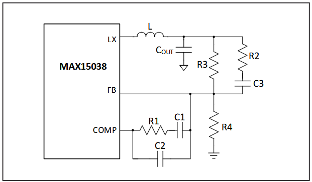
The output voltage of the converter can be set by an external output resistor-divider which comprises R3 and R4 (Figure 4). When externally programming the MAX15038, the output voltage is determined by:
For VOUT = 3.3V, select R3 = 3kΩ, which sets R4 = 665Ω.
Step 6: Compensation Design
The transfer function of the converter comprises one double pole and one zero. The double pole is introduced by the inductor L and the output capacitor CO. The ESR of the output capacitor determines the zero. The double pole and zero frequencies are given in the following equations:
where RL is equal to the sum of the output inductor’s DCR (DC resistance) and the internal switch resistance, RDS(ON). A typical value for RDS(ON) is 24mΩ (LSFET) and 31mΩ (HSFET). The RO is the output load resistance, which is equal to the rated output voltage divided by the rated output current. The ESR is the total equivalent series resistance of the output capacitor.
Since the ESR of ceramic capacitors is typically very low, the frequency of the associated transfer function zero is higher than the unity-gain crossover frequency, fC, and the zero cannot be used to compensate for the double pole created by the output filtering inductor and capacitor. The double pole produces a gain drop of 40dB/decade and a phase shift of 180°. The compensation network error amplifier must compensate for this gain drop and phase shift to achieve a stable high-bandwidth closed-loop system. Therefore, a Type III compensation as shown in Figure 4 is required. Type III compensation possesses three poles and two zeros with the first pole, fP1_EA, located at zero frequency (DC). Locations of other poles and zeros of the Type III compensation are given by:
These equations are based on the assumptions that C1 >> C2 and R3 >> R2 are true in most applications.
Placements of these poles and zeros are determined by the frequencies of the double pole and ESR zero of the power transfer function. It is also a function of the desired closed-loop bandwidth. The following section outlines the step-by-step design procedure to calculate the required compensation components for the MAX15038.
The zero-cross frequency of the closed loop, fC, should be between 10% and 20% of the switching frequency, fS. A higher zero-cross frequency results in faster transient response. Once fC is chosen, C1 is calculated from the following equation:
where VP-P is the ramp peak-to-peak voltage (1V typ). Due to the underdamped nature of the output inductance-capacitance (LC) double pole, the two zero frequencies of the Type III compensation are set less than the LC double-pole frequency to provide adequate phase boost, and the two zero frequencies are set to 80% of the LC double-pole frequency.
Hence:
Setting the second compensation pole, fP2_EA, at fZ_ESR yields:
The third compensation pole is set at 1/2 of the switching frequency. The C2 was calculated using the following equation:
From the above equations, select R1 = 2.7kΩ, R2 = 100Ω, C1 = 4.7nF, C2 = 100pF, C3 = 2.2nF.
Step 7: MODE Selection
The MAX15038 features a mode selection input (MODE) that users can select as a functional mode for the device. This design uses the forced-PWM mode by connecting MODE to GND.
In the forced-PWM mode, the MAX15038 operates at a constant switching frequency (set by the resistor at the FREQ terminal) with no pulse skipping. The PWM operation starts after a brief settling time when EN goes high. The low-side switch turns on first, charging the bootstrap capacitor to provide the gate-drive voltage for the high-side switch. The low-side switch turns off either at the end of the clock period or once the low-side switch sinks to 0.875A current (typ), whichever occurs first. If the low-side switch is turned off before the end of the clock period, the high-side switch is turned on for the remaining part of the time interval until the inductor current reaches 0.58A, or the end of clock cycle is encountered. Starting from the first PWM activity, the sink current threshold is increased through an internal 4-step digital-to-analog conversion (DAC) to reach the current limit of 7A after 128 clock periods. This is done to help a smooth recovery of the regulated voltage even in case of accidental prebiased output despite the initial forced-PWM mode selection.
Step 8: Soft-Start Time Selection
The MAX15038 utilizes an adjustable soft-start function to limit inrush current during startup. An 8μA (typ) current source charges an external capacitor connected to SS. The soft-start time is adjusted by the value of the external capacitor from SS to GND. The required capacitance value is determined as:
where tSS is the required soft-start time in seconds.
This design uses C = 22nF which is equivalent to 1.65ms of soft-start time.
Documentation & Resources
-
MAXREFDES1120 Design Files11/21/2021ZIP829 K
-
MAXREFDES1120: 3.3V/4A Synchronous Step-Down DC-DC Converter Using MAX1503811/21/2021PDF581 K
Support & Training
Search our knowledge base for answers to your technical questions. Our dedicated team of Applications Engineers are also available to answer your technical questions.