Overview
Features and Benefits
- 2-layer Rogers 4350B evaluation board with heat spreader and wideband, surface-mount bias tee circuit
- End launch, 2.92 mm RF connectors
- Through calibration path
Product Details
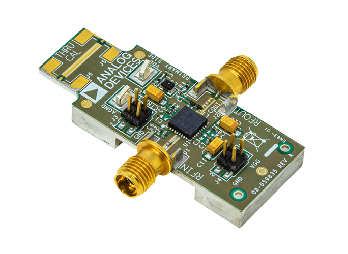
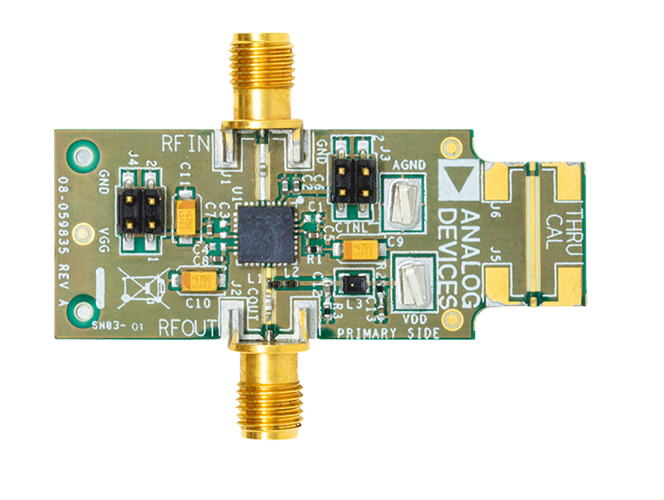
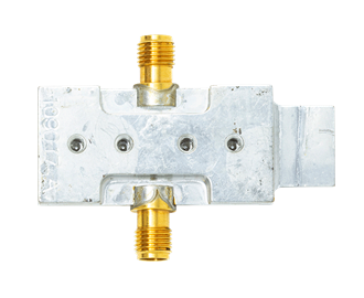
The EV2HMC994APM5 consists of a 2-layer printed circuit board (PCB) fabricated from 10 mil thick, Rogers 4350B, copper clad, mounted to an aluminum heat spreader. The heat spreader assists in providing thermal relief to the device as well as mechanical support to the PCB. Mounting holes on the heat spreader allow it to be attached to a heat sink for improved thermal management. The RFIN and RFOUT ports are populated with 2.9 mm, female coaxial connectors, and their respective RF traces have a 50 Ω characteristic impedance.
The EV2HMC994APM5 differs from the EV1HMC994APM5 in one key respect. Whereas the EV1HMC994APM5 requires an external connectorized bias tee on its RFOUT port to operate (see the HMC994APM5E data sheet for additional details), the EV2HMC994APM5 contains an on-board, surface-mount bias tee circuit. This circuit allows the EV2HMC994APM5 to connect directly to RF test equipment, such as network analyzers and spectrum analyzers. However, this on-board, surface-mount bias tee circuit limits the operating frequency to approximately 22 GHz (see Figure 2 in the user guide). This frequency contrasts with the DC to 28 GHz operating frequency range that is achievable when the HMC994APM5E is operating with a broadband connectorized bias tee. The design and operation of this circuit is discussed in detail in the AN-2061 Application Note.
The EV2HMC994APM5 is populated with components suitable for use over the entire operating temperature range of the HMC994APM5E. To calibrate out board trace losses, a through calibration path, THRU-CAL, is provided between the J5 and J6 connectors. J5 and J6 must be populated with 2.92 mm RF connectors to use the through calibration path. Refer to Figure 3 and Table 2 in the user guide for the through calibration path performance. The power voltages, ground voltages, gate control voltages, and detector output voltages are accessed through two 4-pin headers, J3 and J4 (see Table 1).
The RF traces are 50 Ω, grounded, coplanar waveguide. The package ground leads and the exposed paddle connect directly to the ground plane. Multiple vias are used to connect the top and bottom ground planes with particular focus on the area directly beneath the ground paddle to provide adequate electrical conduction and thermal conduction to the heat spreader.
The decoupling capacitors on the EV2HMC994APM5 represent the configuration used to measure the performance of the circuit, which is detailed in AN-2061. It is possible to reduce the number of capacitors connected to the ACG2, ACG3/ACG4, VGG1, and VGG2 pins, but this reduction varies from system to system. It is recommended to first remove the largest capacitors that are farthest from the HMC994APM5E when reducing the number of capacitors.
For full details on the HMC994APM5E, see the HMC994APM5E data sheet, which must be consulted in conjunction with the user guide when using the EV2HMC994APM5.
Markets and Technologies
Applicable Parts
Getting Started
EQUIPMENT NEEDED
- RF signal generator
- RF spectrum analyzer
- RF network analyzer
- 10 V, 0.5 A power supply
- −1.5 V, 100 mA power supply
Documentation & Resources
-
EV2HMC994APM5 Gerber Files12/10/2024ZIP1 M
-
HMC994APM5E Gerber Files9/28/2017ZIP3 M


