AN-2635: Nikon A-Format® Absolute Encoder Protocol Support for TMC8100
Description
The TMC8100 includes a programmable microcontroller optimized for serial synchronous and asynchronous absolute encoder protocols up to 16Mbit/s. It can replace dedicated encoder protocol interface ICs and field programmable gate array (FPGA) implementations while supporting in-system updates for different encoder capabilities or for switching to other encoder protocols. The TMC8100 is a compact, cost-effective, and flexible communication solution for adding absolute encoder support to industrial drives.
This application note provides details on the TMC8100 software implementation example supporting the absolute position encoder with the A-format® interface.
System Description
Servo motor drives, for example, in industrial applications, typically require accurate, reliable, and low-latency position feedback. For a long time, optical encoders with incremental A/B/N output have been the industry standard. Nevertheless, absolute position encoders are gaining traction, often with additional functionality and different interface protocols (mostly vendor-specific). An example is the A-format protocol from Nikon for serial transfer of digital data between the encoder and controller. The physical layer is based on the RS485 standard and capable of transmitting position values (single turn and multi-turn), diagnostic information, and allows reading and writing of the internal memory of the encoder. It uses half-duplex serial communication.
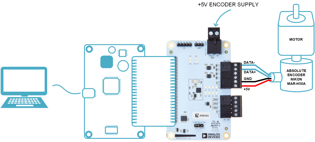
The encoder with the A-format protocol connects to the TMC8100-EVAL-KIT through a single-shielded, six-wire cable (Figure 1). The six wires are as follows:
- +5V and GND: Encoder power supply and ground connection.
- Vbat and GND: Battery power supply (not used with the TMC8100-EVAL-KIT).
- DATA+ and DATA-: Differential RS485 signals for data communication (half-duplex).
The reference implementation features:
- 2.5Mbps data rate as supported by the A-format protocol.
- Send command (example: CDF0) and receive reply.
- Assembly and disassembly of data.
- On-the-fly calculation of CRC checksum and adding to transmit data.
- On-the-fly calculation of CRC checksum and compare with received CRC.
The reference implementation is available as source code. Users may use this as a starting point and apply changes as required by the application.
System Overview
The provided software is designed to operate in conjunction with the TMC8100-EVAL-KIT and tested with the MARH50A encoder from Nikon.
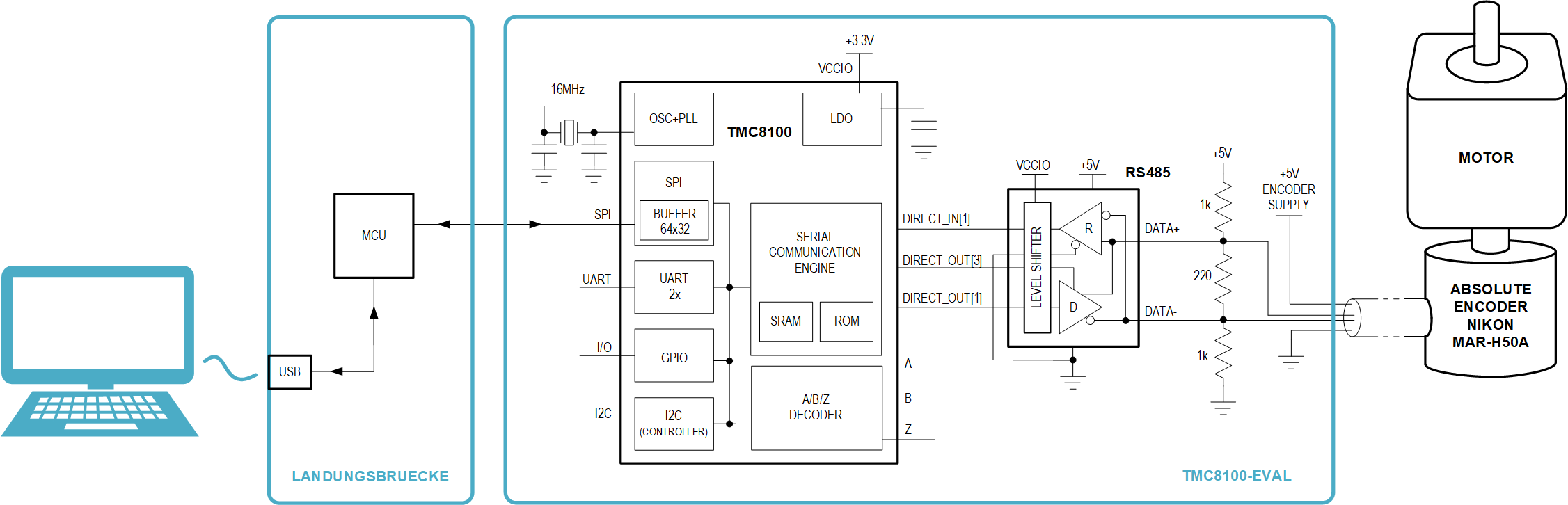
The core hardware components used from the TMC8100-EVAL-KIT are the TMC8100 and one RS485 transceiver for converting between the TMC8100 single-ended input and output signals, and the differential RS485 signals available as DATA+ and DATA- at the connector (Figure 2).
The software includes the firmware for the TMC8100 with the implementation of the controller functionality for the protocol support. This firmware must be downloaded to the TMC8100 after power-up. An additional GUI for selecting and downloading the firmware and demonstrating and testing the functionality of the firmware is available as Python script.
A-Format Protocol
A-format is a communication protocol used for Nikon absolute position encoders. It uses bidirectional, half-duplex serial communication over a single pair of twisted wires (RS485). In addition to reading out the encoder absolute position information, the protocol supports, example, reading status information including encoder temperature, and reading and writing to the encoder internal EEPROM.
Communication with an encoder using the A-format protocol usually comprises a request (command data) sent from the controller to the encoder and a reply from the encoder to the controller before the next request may be sent.
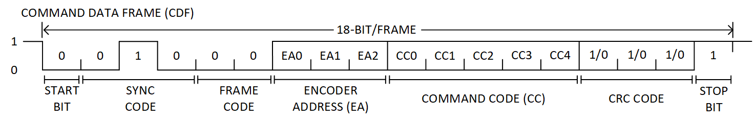
There are several predefined commands available. For requesting the encoder absolute position information, command data frame 0 (CDF0) is used in this example. It consists of a single 18-bit frame sent from the controller to the encoder and four 18-bit frames sent back from the encoder to the controller as a reply (Figure 3).

An 18-bit frame always starts with a START bit (‘0’) and ends with a STOP bit (‘1’). The 16-bit in-between may have different meanings.
For the command data frame (CDF, Figure 4), the START bit is followed by the SYNC code (“010”), FRAME code (“00”), encoder address (EA, default is “000”), command code (CC, “00000” for CDF0), 3-bit CRC code (CRC polynomial p(x) = x^3+x+1, covers frame code, encoder address, and command code), and finally, the STOP bit.
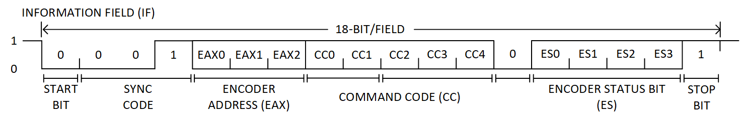
The encoder reply starts with the 18-bit long information field (IF, Figure 5). The START bit here is followed by the SYNC code (always “001”), encoder address (EAX, default is “000”), a copy of the command code from the command data frame (CC, “00000” for CDF0), one fixed bit with value zero (‘0’), encoder status bits (ES), and finally, the STOP bit (‘1’).
Next to the information field, three data fields follow for CDF0. Each data field (Figure 6) contains 16-bit of data (LSB first) between the START and STOP bit.
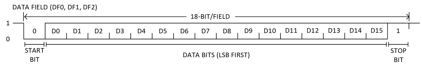
The encoder used in this example transmits 20-bit of single turn (ST), 16-bit of multi-turn (MT) encoder data, and an 8-bit CRC checksum as part of the three data fields (Table 1). For the CRC checksum, the polynomial p(x) = x^8+x^4+x^3+x^2+1 is used. The CRC covers all bits of the reply (IF and DF0..2), except for START and STOP bits.
| Command Data | Encoder Data | |||
| IF | DF0 | DF1 | DF2 | |
| CDF0 | IF[0:2] = “001”, IF[3:5] = EAX, IF[6:10] = CC, IF[11] = ‘0’, IF[12:15] = ES |
D[0:15] = ST[0:15] | D[0:3] = ST[16:19] D[4:15] = MT[0:11] |
D[0:3] = MT[12:15] D[4:7] = “0000” D[8:15] = CRC[0:7] |
For more details on this protocol, including information on the other command data frames refer to the encoder specification from Nikon.
Software Overview
The firmware implementation for the A-format protocol for the TMC8100 is available as source code “tmc8100- eval_A-format_encoder_demo_v10.asm” and as machine code in intel hex file format “tmc8100- eval_A-format_encoder_demo_v10.hex”. For first tests/evaluation of the functionality, a Python script “tmc8100- eval_A-format_encoder_demo_v10.py” is available. This is expected to be executed on a PC connected to the TMC8100- EVAL-KIT through a USB with the encoder attached, as shown in Figure 1.
The Python script program requires a Python interpreter installed on the PC and makes use of the “intelhex” and “pySerial” Python libraries, among others. It uses “tkinter” for the graphical user interface.
After connecting the encoder to the TMC8100-EVAL-KIT, the USB to the PC, and applying +5V to the TMC8100-EVAL-KIT, the Python script may be executed from the command line.

At first, the virtual COM port for the USB connection to the TMC8100-EVAL-KIT must be selected. In this example, it is “COM4.” The lines of output in the terminal window already indicate successful connection to the Landungsbruecke (LB) and detection of the TMC8100 with chip ID and revision number.
Afterwards, the GUI automatically starts in a separate window.

First, the hex file “tmc8100-eval_A-format_encoder_demo_v10.hex” with the example code for the TMC8100 must be selected with the “…” button in the Select Input File frame (1). By pressing Load + Execute (2) as next step, the content of the file is written through the USB and Landungsbruecke/LB into the SRAM program memory of the TMC8100 with the help of the bootloader, and program execution is started. Note that this program comes with its own communication protocol for encoder access. To put the TMC8100 into bootloader mode again, for example, for downloading a different program, a reset or power cycle is required.
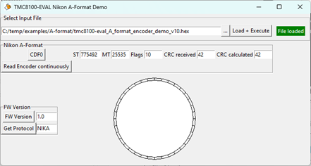
The Nikon A-format frame in the middle of the window offers two command buttons to initiate an encoder readout. Pressing CDF0 instructs the firmware on the TMC8100 to send out the command data frame 0 (CDF0) command to the encoder and read back the absolute encoder position. This position is divided into the absolute position within one rotation/single-turn (next to the label “ST”) and the number of complete rotations/multi-turn (next to label “MT”). In addition, the flags as part of the received information field (IF) are displayed next to the label “Flags”. The last two items in this row are the received 8-bit checksum (next to “CRC received”) and the calculated one from the received data (next to “CRC calculated”). If there is no transmission error, both CRC checksums should be the same.
In parallel to the GUI with the extracted/relevant data, the raw communication data with some additional information is shown in the command line window, which might be helpful when modifying/extending the TMC8100 program example.

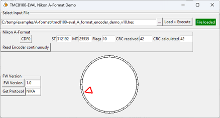
Pressing Read Encoder continuously in the GUI triggers the read-out of the encoder value continuously by the Python program. In addition to an update of the encoder position information (ST and MT values (the other values/flags and CRC are not updated!)), an analog dial-wheel with a red position mark is also updated with the encoder ST value as the indicator for the current absolute 360° angle position (Figure 7). To stop encoder read-out, the Python program must be terminated/restarted.
Output to the command line window is suppressed during continuous encoder read-out for performance reasons.
Firmware Implementation
The example source code “tmc8100-eval_A-format_encoder_demo_v10.asm” may be used as the starting point and modified according to application requirements. An assembler is available for translation of the source code (Assembler).
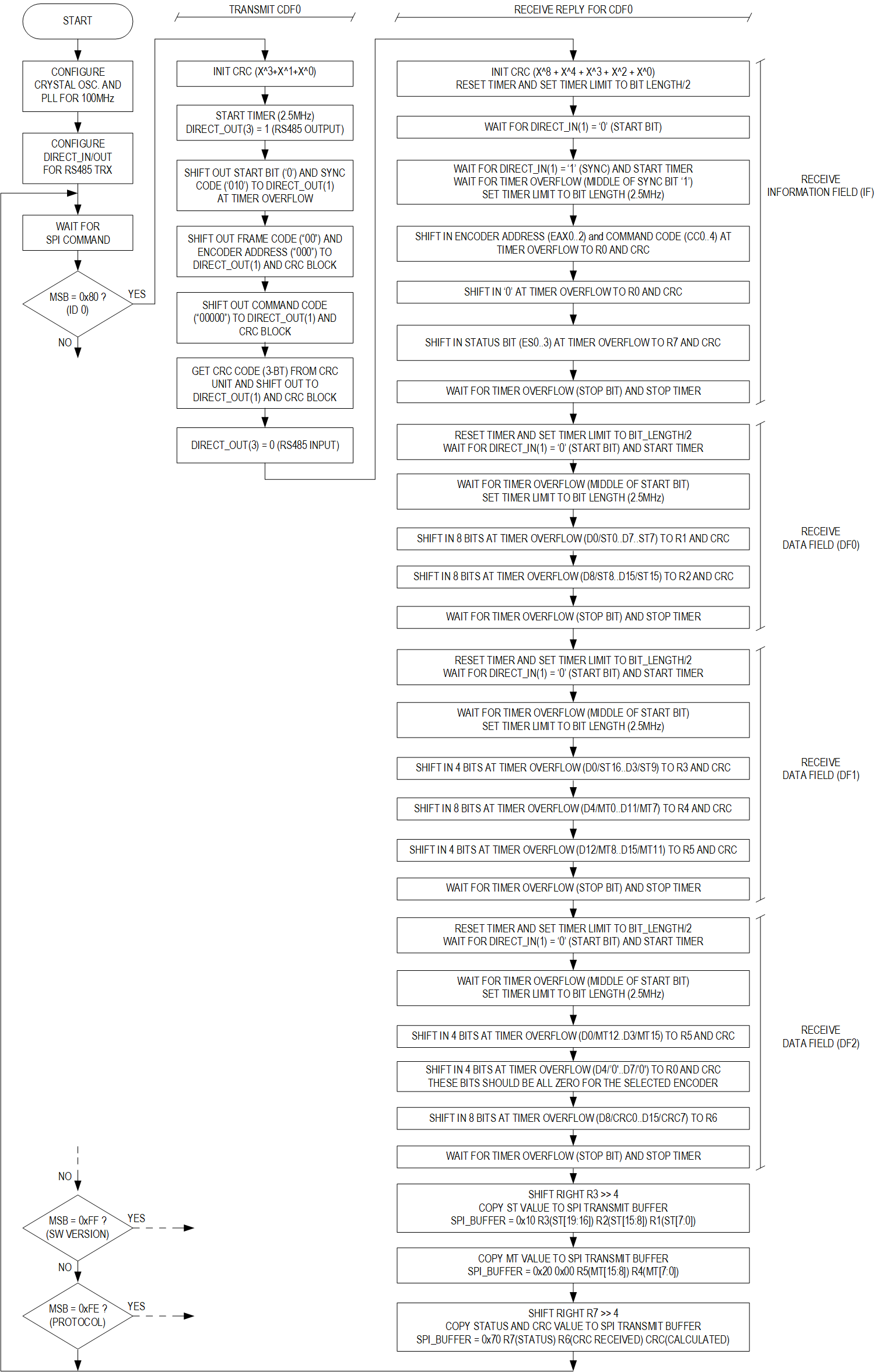
The flowchart (Figure 9) gives an overview of the example code for the command data frame 0 (CDF0) and capturing the reply from the encoder.
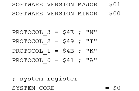
The firmware source code starts with the definition of some values (example, software version and protocol supported) and the register addresses of peripheral units inside the TMC8100 for better readability (Figure 8).
SPI Configuration
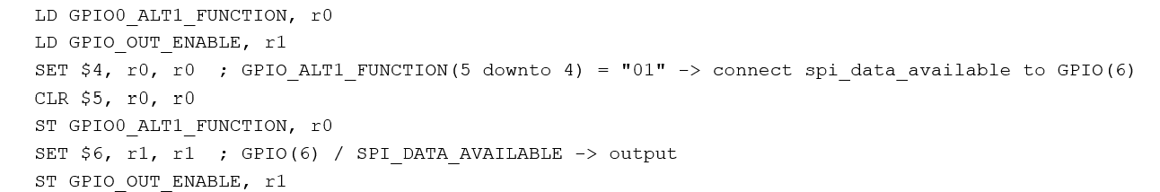
The standard SPI signals (SPI_CSN, SPI_SCLK, SPI_SDI, and SPI_SDO) available with the TMC8100 do not require any configuration. They have fixed functionality and pin assignment for the package. Nevertheless, an additional signal, SPI_DATA_AVAILABLE, is available that can be configured as an alternate function of pin GPIO(6) and indicates (output high ‘1’) data written to the SPI output buffer by the firmware inside the TMC8100. This allows for feedback/interrupt to the attached microcontroller, which may then initiate an SPI datagram/transaction to fetch the reply data for a previously transmitted command from the TMC8100. This functionality is already configured by the bootloader after power-up and is included here for completeness (Figure 10).
Clock Selection and Initialization
The TMC8100 always starts running on the internal oscillator and the bootloader configures the PLL for a system clock frequency of 75MHz after power-on/reset. In this example, the crystal oscillator is used with the 16MHz crystal available on the TMC8100-EVAL-KIT. In case there is already a precise/crystal oscillator generated clock available in the application circuit, this clock may be used instead and connected to GPIO0/external clock input (CLK_EXT). The PLL output and system frequency is set to 100MHz to simplify clock calculation/divider settings afterwards. The PLL can be set to a maximum of 128MHz.
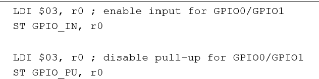
As first step, pins GPIO0 and GPIO1 are configured for an external crystal in combination with the internal crystal oscillator (Figure 11).
Next, the PLL feedback divider is configured for 100MHz PLL output frequency (PLL_FB_100), and the clock circuitry for the crystal oscillator (XTAL) and the PLL input divider set to get 1MHz clock frequency at the input of the PLL (Figure 12). As the clock block is addressed indirectly, four commands are necessary for each register write access: a pair of load (LDI) and store (ST) instructions to set the register address and another pair of load and store instructions to set the register value.
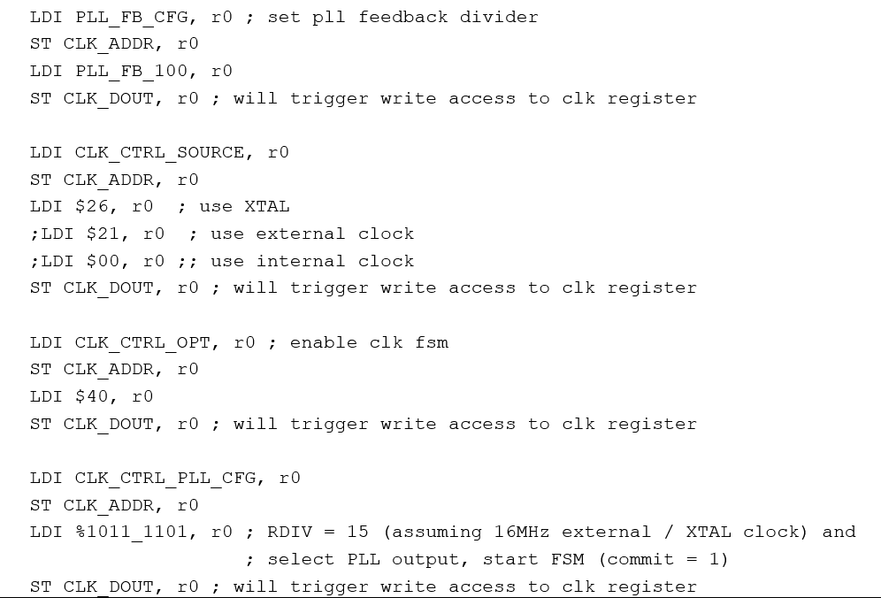
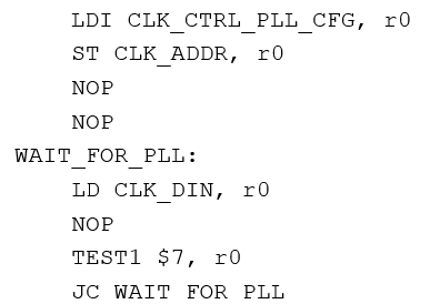
The last write access triggers the internal state machine of the clock block to apply all changes. As this includes the start-up of the crystal oscillator and waiting for the PLL to lock, it is necessary to poll the status register of the clock block and wait until the new 100Mhz system clock is stable and available (Figure 13). Therefore, the address of the configuration register (CLK_CTRL_PLL_CFG) is written to the address register of the clock block (CLK_ADDR) and the program reads out this register in a loop until bit 7 (TEST1 $7, r0) is cleared and the new clock is available.
DIRECT_IN / DIRECT_OUT Pin Configuration
Figure 2 shows that only one RS485 transceiver on the TMC8100-EVAL-KIT is required for communication with the encoder. Transmit enable of the RS485 transceiver is connected to signal DIRECT_OUT(3) and transmit data is shifted out through DIRECT_OUT(1). The RS485 receiver is permanently enabled and data is received/shifted in using DIRECT_IN(1).
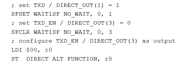
At start, the transmit output (DIRECT_OUT(1)) is set to ‘1’ (idle state), the RS485 transmitter enable control signal (DIRECT_OUT(3)) is set to ‘0’ (receive mode) and configured as output (Figure 14).
SPI Command Loop
After the configuration of the TMC8100, the program waits for commands received through the SPI from an external MCU in an endless loop. All SPI transactions are expected to be 32-bit datagrams. All commands of this example code fit into one datagram. For simplification, just the upper 8-bit (MSB, received first through SPI) are tested for command selection and execution. The command loop starts with reading out the status register (SPI_STATUS) of the SPI peripheral block and waiting until bit 0 of the status register changes to one (WAIT1 $0, r0), indicating an SPI datagram is received and is available in the SPI input buffer (SPI_BUFFER).
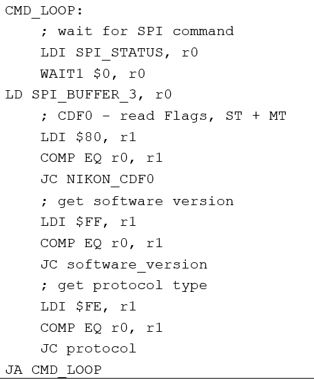
The upper 8-bit of the contents of the 32-bit SPI input buffer are compared against $80 (the SPI command defined in this example code for reading out the encoder data incl. flags and position value). If this comparison is successful, program execution jumps to address “NIKON_CDF0”. With the program code at this address (described in more detail as following), the attached RS485 transceiver is switched to transmit mode and the CDF0 18-bit long command data frame is shifted out using DIRECT_OUT(1). After switching back to receive mode, the reply data from the encoder (information field (IF) and data fields (DF0 … DF2)) is shifted in using DIRECT_IN(1). The received data is then extracted and assembled into three 32-bit SPI datagrams, one with the single turn data (ST), one with the multi-turn data (MT), and one with flags and CRC, and written to the SPI output buffer. As the output buffer gets filled up, the signal SPI_BUFFER_AVAILABLE/GPIO6 changes from low ‘0’ to high ‘1’, indicating new data available for SPI transaction. With the next SPI transaction(s), this data can be read out. It is expected that a new command is not sent before all data from the previous command is read out. As one SPI transaction always transfers data in both directions and there is usually more than one transaction necessary to read out all reply data, it is recommended to use a “dummy” command (example, 0x00 0x00 0x00 0x00), which is not interpreted by the command loop for these additional read-outs. The last transaction for read-out may already include the next command.
The Python script available to test the encoder implementation “tmc8100-eval_nikon_A-format_demo.py” with the TMC8100-EVAL-KIT offers a GUI with a “Read Encoder” push button. Pressing this instructs the Landungsbruecke (LB) to send out an SPI datagram 0x80 0x00 0x00 0x00 (Figure 16 - extract from “tmc8100-eval_nikon_A-format_demo.py”) to the attached TMC8100 on the evaluation board.
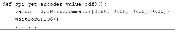
Afterwards, the program waits for a reply from the encoder. The pin SPI_DATA_AVAILABLE/GPIO6 switches from low (‘0’) to high (‘1)’ as soon as the reply data is available in the SPI output buffer of the TMC8100. For reading out this data, the Python program uses the SPI “dummy” commands 0x00 0x00 0x00 0x00 not interpreted by the TMC8100 firmware (Figure 17).
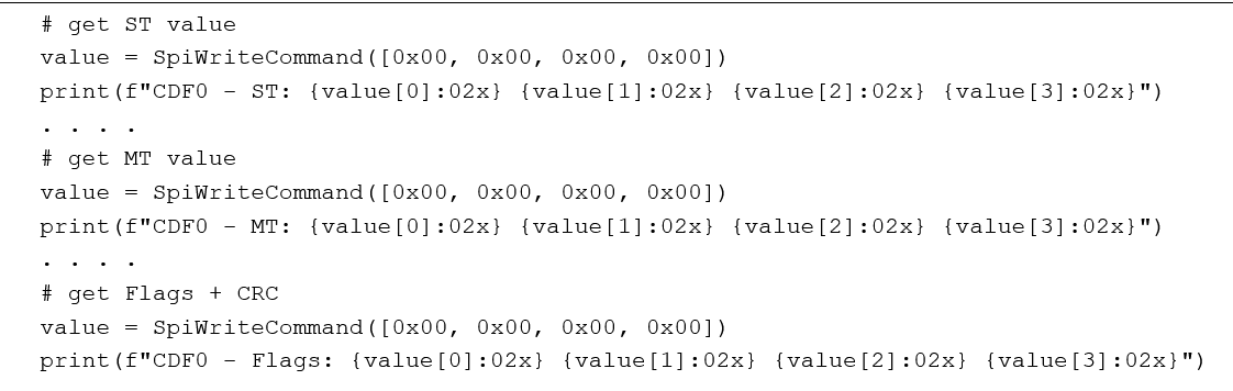
The following table provides an overview of all the SPI commands supported by the example program and reply data available in return. SPI commands always fit into one 32-bit datagram while the reply may take up-to 3x 32-bit datagrams in this example. SPI 32-bit datagrams are given as four consecutive hex numbers (one hex number per byte with the MSB first for better readability). For the reply, the 32-bit datagrams are shown in the order they are put into the SPI transmit buffer/can be read out (first-in first-out (FIFO)).
| SPI-COMMAND (32-BIT) | SPI-REPLY (32-BIT) |
| 0x80 0x00 0x00 0x00 Read encoder absolute position value within one rotation (ST) and flags/status/information. |
1. 0x10 0x0 ST19 .. ST0 (Single turn encoder position ST19 .. ST0) 2. 0x20 0x00 MT15 .. MT0 (Multi-turn encoder position MT15 .. MT0) 3. 0x70 0x0 Flags CRC(RX) CRC(CALC) Flags ES3 .. ES0 and CRC (Received and calculated) |
| 0xff 0x00 0x00 0x00 Get firmware version. |
1. 0xff 0x00 VERSION_MAJOR VERSION_MINOR |
| 0xfe 0x00 0x00 0x00 Get encoder protocol. |
1. 0x4E (“N”) 0x49 (“I”) 0x4B (“K”) 0x41 (“A“) |
When pushing “Read encoder continuously”, the first command in the table 0x80 0x00 0x00 0x00 is sent repeatedly by the Python program in an endless loop.
CDF0 Request
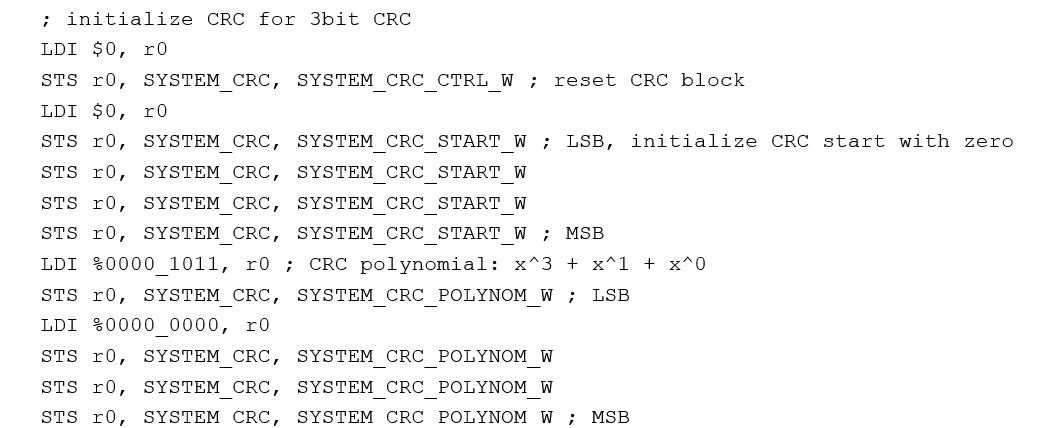
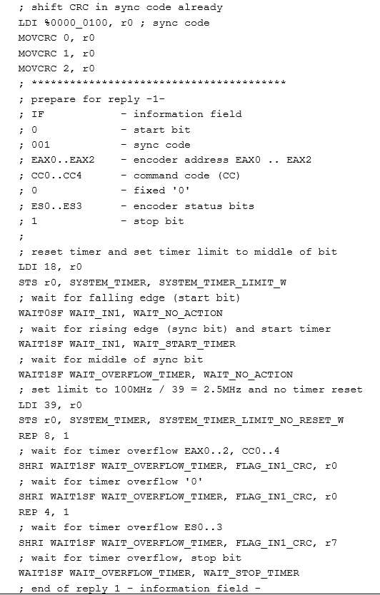
As soon as a new SPI command is received while the TMC8100 software is waiting for SPI commands and the upper byte/the byte received first within the 32-bit datagram is equal to $80, the program execution jumps to address “NIKON_CDF0” in program code. The program code at the target address starts with initializing the CRC block for on-the-fly CRC calculation for the 3-bit CRC code transmitted as part of the command CDF0 (Figure 18) . The CRC polynom is set to P(x) = x^3 + x^1 + x^0 and the start value is set to zero.
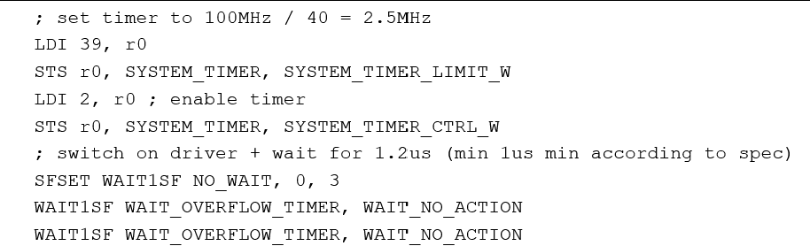
For the encoder protocol and the encoder used in this example, the required transmission data rate is 2.5Mbit/s. As the internal system clock is set to 100MHz, the system timer used for shifting out the bits is set to 39 to get to a division factor of 100MHz/40MHz = 2.5MHz (Figure 19). Afterwards, the timer is enabled and the external RS485 driver is switched to transmit mode setting DIRECT_OUT(3) output to ‘1’ (SFSET WAIT1SF NO_WAIT, 0, 3).
After waiting some time for the output of the RS485 transceiver to stabilize the start bit (“0”) and 3-bit sync code (“010”) is shifted out from system register r0 on DIRECT_OUT(1) using the SHRO instruction (Figure 20)(Figure 21). This instruction is executed four times using REP 4, 1. For each loop instruction, execution is suspended until the system timer wraps around (parameter WAIT_OVERLFLOW_TIMER) before shifting out the new LSB from register r0 to DIRECT_OUT(1). Afterwards, the 2-bit frame code (“00”) and the 3-bit encoder address (“000”) are shifted out in a similar manner, preloading register r0, and repeating the SHRO instruction five times using REP 5, 1. This sequence is followed by another 5-bit for the command code, which is also all zero (“00000”) for CDF0.
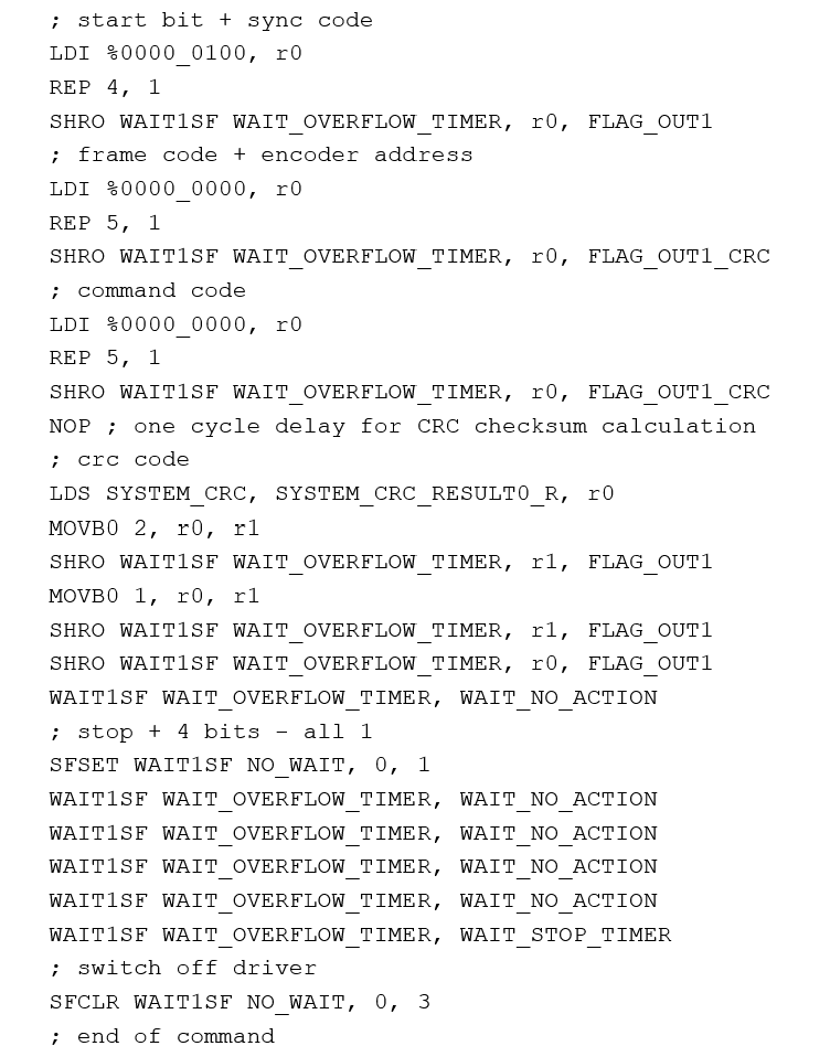
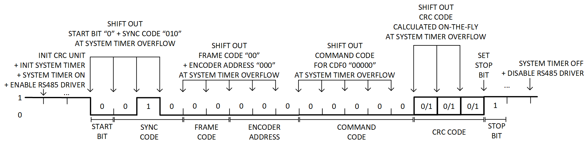
All bits shited out to DIRECT_OUT(1) starting with the frame code are at the same time shifted into the CRC unit for CRC calculation using parameter FLAG_OUT1_CRC instead of FLAG_OUT1.
As last part of the command frame, the 3-bit CRC code is shifted out. The calculated CRC code is loaded from the CRC unit (SYSTEM_CRC_RESULT0) and the relevant bits brought into the correct order one by one using bit move instruction MOVB0. Using the CRC block for calculation of the the CRC value simplifies CRC calculation in case parts of the command have to be adapted for the application (example, different encoder address).
The DIRECT_OUT(1) serial output is then set to “1” for the stop bit (SFSET WAIT1SF NO_WAIT, 0, 1), and finally, DIRECT_OUT(3) switched low to turn off the RS485 transceiver and prepare for receiving data from the encoder.
CDF0 Reply
To prepare for the reply from the encoder, the CRC calculation block is initialized to enable on-the-fly CRC calculation while the serial data is shifted in.
 ; initialize CRC for 8bit CRC
 LDI $0, r0
 STS r0, SYSTEM_CRC, SYSTEM_CRC_CTRL_W ; reset CRC block
 LDI %0001_1101, r0 ; CRC polynomial: x^8 + x^4 + x^3 + x^2 + x^0
 STS r0, SYSTEM_CRC, SYSTEM_CRC_POLYNOM_W ; LSB
 LDI %0000_0001, r0 ; CRC polynomial: x^8 + x^4 + x^3 + x^2 + x^0
 STS r0, SYSTEM_CRC, SYSTEM_CRC_POLYNOM_W
 LDI %0000_0000, r0
 STS r0, SYSTEM_CRC, SYSTEM_CRC_POLYNOM_W
 STS r0, SYSTEM_CRC, SYSTEM_CRC_POLYNOM_W ; MSB
First, the linear feedback shift register (LFSR) used for CRC calculation is reset and the polynom used for CRC for this protocol is loaded into the system CRC register (SYSTEM_CRC_POLYNOM_W). This register is 32-bit in size and filled with four write accesses after CRC block reset with one byte after the other in consecutive order starting with the LSB. Bit 0, bit 2, bit 3, bit 4, and bit 8 of the 32-bit register must be set to configure the generator polynomial (x^8 + x^4 + x^3 + x^2 + x^0) used for the encoder reply.
The program then prepares for the first datagram from the encoder (information field (IF)) (Figure 22, Figure 23).
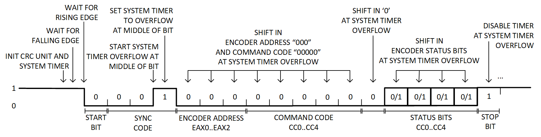
The system timer is configured and the program waits (WAIT0SF) for the falling edge of the start bit from the encoder on DIRECT_IN(1). The IF datagram starts with a 3-bit sync code (“001”). The program waits for the rising edge of the ‘1’ in the sync code and immediately starts the timer, which overflow at the middle of this ‘1’ bit. The system timer limit is then adjusted without resetting the timer counter (limit set to 39 instead of 18) to overflow after one bit length (in the middle of the following bits with 2.5Mbit/s serial data rate). The three sync bits are already part of the CRC checksum. Therefore, these three bits are already shifted into the CRC unit after the configuration of the unit and before the actual data transfer starts using the MOVCRC command.
After the sync code, the three encoder address bits EAX0...EAX2 and five command code bits CC0...CC4 are shifted into register r0 and at the same time into the CRC unit. A fixed ‘0’ bit is shifted in and finally four encoder status bits ES0…ES3 before the stop bit are received and the timer is stopped. This is the end of the first datagram from the encoder.
This first datagram is followed by three more datagrams with a 16-bit datafield each (DF0, DF1, and DF2) containing the 20-bit single-turn encoder position, 16-bit encoder multi-turn information, and 8-bit CRC checksum.
For the datafield datagram, the program initializes the system timer again and waits for the falling edge of the start bit from the encoder (WAIT0SF) to start the system timer (Figure 24, Figure 25). The timer limit is set to overflow at the middle of the start bit. With the overflow, the timer limit is adjusted to overflow the next time at the middle of the next bit (limit set to 39 for 2.5Mbps serial data rate and 100MHz internal clock). With these timer settings, the next 8-bit (encoder position LSB ST0...ST7) are sampled and shifted into register r1, and at the same time into the CRC unit and another 8 bits (encoder position ST8..ST15) into register r2 and the CRC unit in parallel. Finally, with the next timer overflow, the stop bit is received and the system timer stopped.
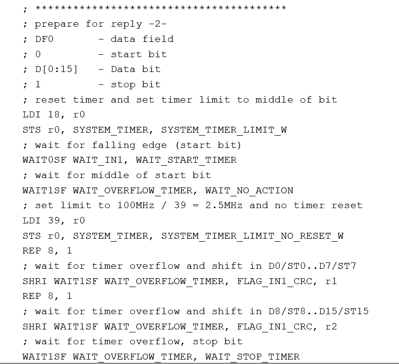
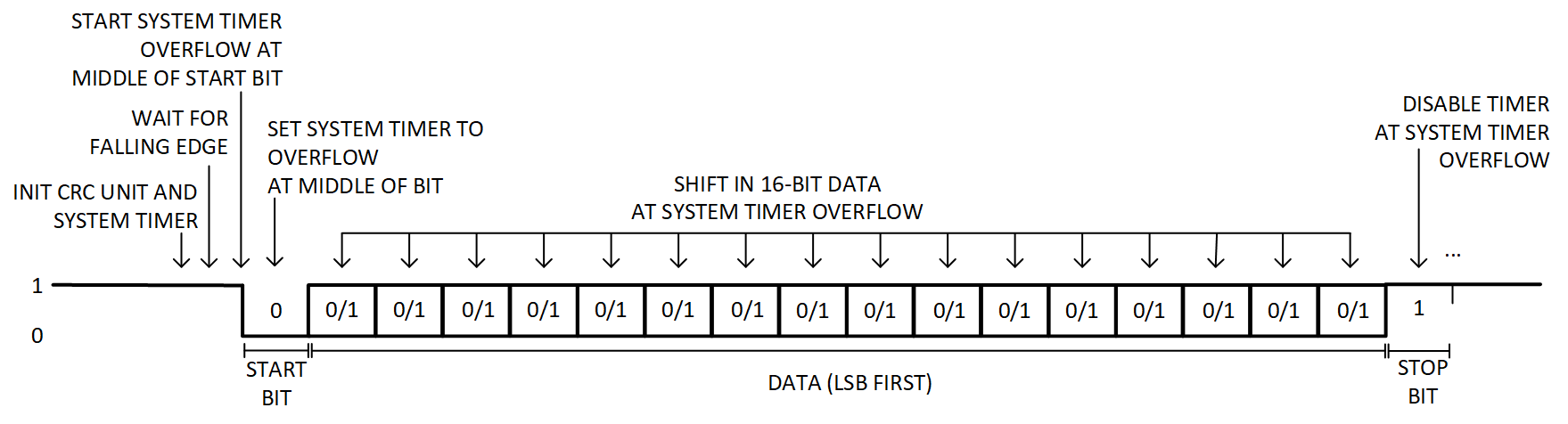
Similar program sequences are used for the next two data fields, DF1 and DF2. With DF1, the upper four bits of the encoder position ST16…ST19 are received and stored in register r3. These are followed by 12-bit of the multi-turn encoder position with the lower 8-bit (MT0…MT7) stored in register r4 and another 4-bit (MT8...MT11) in register r5. Finally, DF2 contains the upper 4-bit of the multi-turn encoder position (MT12...MT15) stored in r6, the next 4-bit unused (all zero), and finally, the 8-bit CRC checksum.
SPI Reply Datagram
All data received and calculated is now available. As next step, these values are copied to the SPI buffer for read-out by the attached microcontroller/motion controller.
The first 32-bit SPI datagram is filled up with the single turn (ST) absolute position information copied to the lower 20-bit and a fixed value of 0x10 as MSB. The upper 4-bit of the ST value in processor register r3 are shifted right first and then copied to the SPI transmit buffer. The lower 16-bit are copied directly from processor registers r1 (LSB) and r2 to the SPI transmit buffer. When the SPI datagram is read out, this fixed MSB value can be used to clearly identify the contents of this datagram.
 ; ST / Single turn value
 LDI %0001_0000, r0
 ST SPI_BUFFER_3, r0
 SHRI WAIT1SF NO_WAIT, FLAG_IN3, r3
 SHRI WAIT1SF NO_WAIT, FLAG_IN3, r3
 SHRI WAIT1SF NO_WAIT, FLAG_IN3, r3
 SHRI WAIT1SF NO_WAIT, FLAG_IN3, r3
 LDI %0000_1111, r0
 AND r3, r0, r3
 ST SPI_BUFFER_2, r3
 ST SPI_BUFFER_1, r2
 ST SPI_BUFFER_0, r1
The second 32-bit SPI datagram is filled up with the multi-turn (MT) position information in the lower 16-bit (rom processor registers r4 and r5 and a fixed value of 0x20 as MSB).
 ; MT / Multiturn value
    LDI %0010_0000, r0
    ST SPI_BUFFER_3, r0
    LDI $0, r0
    ST SPI_BUFFER_2, r0
    ST SPI_BUFFER_1, r5
    ST SPI_BUFFER_0, r4
Finally, the third 32-bit SPI datagram contains a fixed value of 0x70 as MSB, received status flags from processor register r7, CRC checksum value received in register r6, and as LSB, the calculated CRC value from the system CRC unit. The four status flags in register r7 are shifted right first to align within the lower four bits of the byte.
; CRC values + flags
   LDI %0111_0000, r0
   ST SPI_BUFFER_3, r0
   ; status flags SF
   SHRI WAIT1SF NO_WAIT, FLAG_IN3, r7
   SHRI WAIT1SF NO_WAIT, FLAG_IN3, r7
   SHRI WAIT1SF NO_WAIT, FLAG_IN3, r7
   SHRI WAIT1SF NO_WAIT, FLAG_IN3, r7
   LDI %0000_1111, r0
   AND r7, r0, r7
   ST SPI_BUFFER_2, r7 ; status flags
   LDS SYSTEM_CRC, SYSTEM_CRC_RESULT0_R, r0
   ST SPI_BUFFER_1, r6 ; received CRC
   ST SPI_BUFFER_0, r0 ; calculated CRC
Appendix
Assembler
For program development and modification of the examples/reference programs for the TMC8100, an assembler is available. This PC-based command line tool expects as parameter the file name and optional path of the assembler source code file. In case the file with the provided file name is not found, the ending *.asm is added automatically to the provided file name. From this input file, the assembler generates the output file(s).

In this example, the name of the input file with the assembly source code is "tmc8100-eval_abn_demo.asm". The number of machine instructions (16-bit) generated from this file is 83, which is 4.1% of the available program memory (SRAM). The size of the program memory in the TMC8100 is 2K × 16-bit (a maximum of 2048 instructions).
There is one generated default output file that has the name of the input file with *.hex as extension instead of *.asm. This output file is a text file with the program code in standard intel hex file format, example, for loading the program code into the program memory of the TMC8100 on the TMC8100-EVAL-KIT using the TMCL-IDE or one of the Python scripts available with the example code.
The assembler also supports a number of flags for generating additional output files in different formats and additional information.

- Option “-i”: file “<filename>.i” is generated as output from the preprocessor. Contains the contents of the assembly source file with all preprocessor commands (# ...) being processed (example, “#include” file contents merged into the source file) and comments (example, /* .. */ | // | ;) removed.
- Option “-l”: file “<filename>.log” is generated with the assembly source code (without comments and preprocessor commands) with additional instruction encoding and the program memory address of the instructions.
- Option “-c”: file “<filename.c>” is generated with C-code to support program development for the controller used to bootstrap the TMC8100. This file contains an array of integer numbers with the generated machine code.
- Option “-m”—machine flag. For support of different implementations/instruction set (default is TMC8100).
- Option “-h”—print help test as shown in the screenshot
Syntax/Commands Supported
The assembler currently supports all TMC8100 instructions as described in the TMC8100 data sheet.
Preprocessor Commands
Comments
The preprocessor removes all comments from the input file(s) for further processing. Currently, the following options are supported:
- /* <comment> */ - block comment - can include more than one line (C-language style)
- // <comment> - comment until end of line (C/C++ - language style)
- ; <comment> - comment until end of line
#include
#include "<filename>"—contents of file given with name and optional path in <filename> is inserted at the position of the #include preprocessor directive for further processing. The line with the #include directive is removed.
Note: Only quotation marks are allowed around <filename> and there should be no other commands/assignments within this line as they are removed/ignored from further processing.
#define
#define <label> [<replacement text>]
The preprocessor replaces any <label> found in the source file (+ files included with the #include statement) after this command with <replacement text>). As replacement text, the character sequence after <label> separated with at least one space from <label> until end of line (or start of comment) is taken. Only comments and text in quotation marks are excluded from automatic replacement. Label(s) may be redefined afterwards in the source file using another #define with the same <label>.
It is possible to define a <label> without replacement text. In this case, the replacement text is empty. This might be useful, example, in combination with the conditional #ifdef / #ifndef preprocessor commands.
#ifdef, #ifndef, #else, #endif
#ifdef <label> <code block 1> #else <code block 2> #endif
In case <label> is defined earlier, the contents of <code block 1> are interpreted and assembler output generated and <code block 2> is ignored. The intermediate file (“<filename>.i”) just shows <code block 1> and not <code block 2>. The code blocks may contain several lines of assembler instructions, and more. In case <label> is not defined, it is the other way round.
#ifndef <label> <code block 1> #else <code block 2> #endif
In case <label> is defined earlier, the contents of <code block 2> are interpreted and assembler output generated and <code block 1> is ignored. The intermediate file (<filename>.i) just shows <code block 2> and not <code block 1>. The code blocks may contain several lines of assembler instructions, and more. In case <label> is not defined, it is the other way round.
Note: It is sufficient to mention the <label> name before using #define <label>. It is not necessary to provide a replacement text/value.
The #else part is optional. #ifdef or #ifndef blocks may be nested.
Assembler Commands
Numbers
To simplify specification of numbers as binary, decimal, and hexadecimal, different formats are supported. These are as follows:
0x123.. or $123.. are interpreted as hexadecimal numbers (character expected: 0 to 9, a to f or A to F).
%1010.. is interpreted as binary number (characters expected: 0 and 1). The character '_' can be inserted for better readability (example, %1010_0011 for an 8-bit number).
123.. is interpreted as decimal number (characters expected: 0 to 9).
Identifiers
Identifiers may be used for better readability instead of numbers. Identifiers must start with a letter (a to z/A to Z) or '_'. Afterwards, numbers are also allowed (0 to 9). Note that character names are not case sensitive.
Identifiers may be assigned a value using the equal sign. For example,
SPI_BUFFER_0 = $30
Some names should not be used as identifiers:
Assembler instructions. This includes all names listed in the TMC8100 data sheet and also the instruction names preceded with a 'C' (indicating conditional execution of the command).
Identifier r0...r7 are predefined as register 0...7 for specifying all general-purpose registers available.
Labels and identifiers should not have the same name.
Labels
Labels are used as placeholders for program memory addresses. Labels do not have to be assigned a value. They are initialized with the current program memory address while the assembler translates the assembly source into machine code.
Example for an endless loop:
WAIT:
  JA WAIT
Note the ':' character after the label name. The assembler automatically initializes the label WAIT with the program memory address of the next instruction (which, in this case is the JA WAIT command). Jump backs (as shown above), where the label is initialized before it is actually used as part of an instruction and jump forwards (where the label is initialized after it is referenced with an instruction) are both supported.