AN-1535: ADuM4135 Gate Driver Performance Driving SiC Power Switches
Introduction
In solar photovoltaics (PV) and energy storage applications, there is a trend towards increased power density along with the ever present need of improved efficiency. A solution to this problem comes in the form of silicon carbide (SiC) power devices.
SiC devices are wide band-gap devices that can operate at an increased voltage of >120 V dc and tend to have a low drain source impedance (RDSON). With some devices having an RDSON as low as 8 mΩ, these devices also fill the need for reduced conduction losses and therefore increased efficiency. SiC devices can also exhibit fast switching speeds of >100 kHz with low parasitic capacitance and associated charge during switching. However, disadvantages include a requirement for higher common-mode transient immunity (CMTI) greater than 100 kV/μs required for gate drivers. Another disadvantage is that higher switching across the drain source of the SiC can lead to ringing at the gate of the device. These disadvantages can cause problems when driving higher voltage SiC devices, where significant power density improvement can be achieved by their implementation.
One combination of gate driver and SiC that can solve these problems is the ADuM4135 and the SiC module, as specified in Table 1. The power module is a half bridge SiC device with a 1200 V collector emitter voltage rating and a continuous current capability of 75 A. Its gate source voltage (VGS) rating is +20 V to −10 V. It has an isolation rating of 2.5 kV for 1 min. The input capacitance (CISS) of the modules is 4.2 nF, with a reverse recovery time of 25 ns.
The ADuM4135 gate driver is a single-channel device with a typical drive capability of 7 A source/sink at a 25 V operating voltage (VDD to VSS). It has a minimum CMTI of 100 kV/μs.


Experimental Setup
Measuring Gate Drive Signals
For high voltage measurement, differential probes are typically used to isolate the user from the high voltage measurement. However, these probes tend to be noisier than standard passive probes and can distort the measurements. Figure 2 shows the difference between the isolated probe and the passive probe when measuring at the same point. For these measurements, the high-side measurement is achieved by isolated probes where there is a need for isolation to higher voltages. However, for the low-side measurement, a standard passive probe is used to obtain a more accurate representation of the signals present. Figure 3 shows how this measurement is achieved, and Figure 2 shows the corresponding result. The signals are as follows:
- VGS is the voltage measured directly at the gate source pins of the power device.
- VDS is the voltage measured at the drain source of the power device.


Gate Voltage Control
At the beginning of the tests, it was observed that the gate to source voltage had a sharp rise time, which can cause issues because it creates a restrictive electromagnetic interference (EMI) environment. Therefore, it was decided to soften the switching by adding a 4.7 nF capacitor on the gate. This capacitor was added directly at the pins of the module between gate and source. Figure 4 and Figure 5 show the VGS gate drive signal prior to adding the capacitor; a sharp slew rate is shown. Figure 5 is a zoomed in view of Figure 4. Figure 6 shows the response with the capacitor added at the gate, where a more controlled rise time is shown at the VGS.


Decoupling the DC Link
Initially, a 10% to 20% ripple was observed on the dc bus on the dc input voltage when switching. This ripple is shown in Figure 7. To reduce this ripple, extra capacitance to a total of 1100 μF was added to improve the decoupling on the dc bus.


Test Setup
Electrical Setup
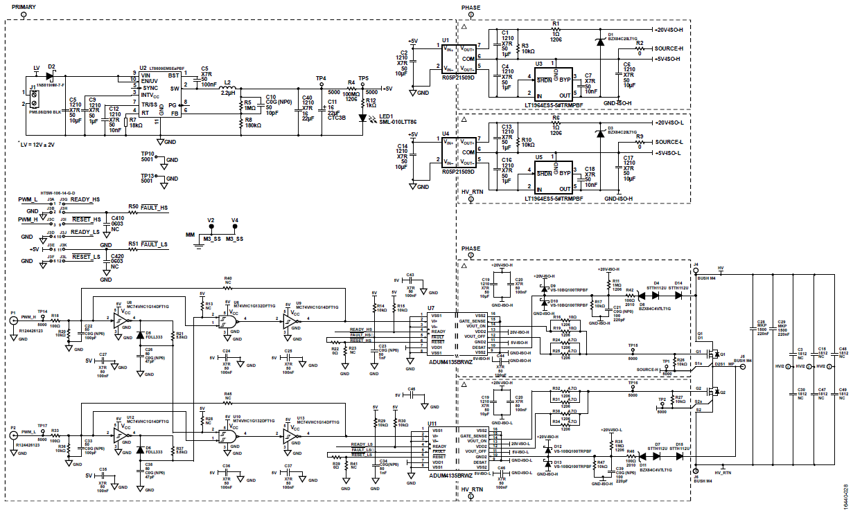
The setup of the system test circuit is shown in Figure 8. A dc voltage is applied to the inputs, which is across the full half bridge, where decoupling capacitors of 1100 μF are added to the input stage. The output stage is an inductor capacitor (LC) filter stage of 200 μH and 128 μF, filtering the output into the load, R1, of 2 Ω to 3 Ω. Table 1 shows a list of the test setup power components. A complete setup is shown in Figure 9, and Table 2 shows the full list of equipment used in the test.


| Equipment | Value |
| U1 | 200 V to 900 V |
| C1 | 1100 μF |
| L1 | 200 μH |
| C2 | 128 μF |
| R1 | 2 Ω to 3 Ω |


| Equipment | Manufacturer | Type |
| Oscilloscope | Agilent | DSO-X 3034 |
| DC Supply | Delta Elektronika | SN660-AR-11 (two in serial) |
| Gate Driver Board | Watt&Well | ADUM4135-WW-FJ-01 SN07 |
| Waveform Generator | Agilent | 33522A |
| Current Probe | Hioki | 3275 |
| Passive Voltage Probe | Agilent | N2863B 300MHz |
| Passive High Voltage Probe | Elditest | GE3421 100MHz |
Test Results
No Loading Testing
The ADuM4135 is in its first revision released (AA). One change was made: a capacitor of 4.7 nF was added on the gates of the power metal-oxide semiconductor field effect transistors (MOSFETs), Q1 and Q2. Table 3 and Table 4 are a summary of the results observed, and Figure 10 through Figure 15 show the proof of results. Test 1 and Test 3 were carried out at 600 V and 900 V, respectively, at a 50 kHz switching frequency, whereas Test 2 was carried out at 600 V at a switching frequency of 100 kHz.


| Test | VDC (V) | Switching Frequency, fsw (kHz) | Duty Cycle (%) | DC Loss (W) | Figures |
| 1 | 600 | 50 | 50 | 30 | Figure 10 and Figure 11 |
| 2 | 600 | 100 | 50 | 66 | Figure 12 and Figure 13 |
| 3 | 900 | 50 | 50 | 63 | Figure 14 and Figure 15 |
| Test | VDC (V) | fsw (kHz) | Ambient Temperature (°C) |
Heatsink Temperature (°C) |
DC-to-DC Power Supply Temperature, High-Side (°C) |
DC-to-DC Power Supply Temperature, Low-Side (°C) |
Gate Driver Temperature, High-Side (°C) |
Gate Driver Temperature, Low-Side (°C) |
| 1 | 600 | 50 | 30 | 57 | 57 | 58 | 57 | 57 |
| 2 | 600 | 100 | 30 | 67 | 60 | 61 | 65 | 66 |
| 3 | 900 | 50 | 30 | 70 | 61 | 61 | 65 | 65 |


Load Testing
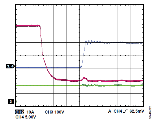
The ADuM4135 is in its first revision released (AA). One change was made: a capacitor of 4.7 nF was added on the gates of the power MOSFETs, Q1 and Q2. Similar to the test setup of the no load tests in the previous section, Table 5 is a summary of the results observed, and Figure 16 through Figure 27 show the proof of results. Test 4, Test 5, and Test 6 were carried out at 200 V at a 50 kHz switching frequency with a 25% duty cycle, whereas Test 7 was carried out at 600 V at a 50 kHz switching frequency with a 25% duty cycle. Test 8 and Test 9 were carried out at 900 V at 50 kHz and 100 kHz switching frequencies, respectively.
The output current (IOUT) was measured at the output of R1, the output load resistor, whereas the output voltage (VOUT) was measured as the voltage across R1. The test results show some Miller feedback on VGS, but VGS remains at the −4 V level at the gate of the SiC. At 900 V, some ringing is seen on VDS, but it is <30 V of the input dc voltage. This design shows how the ADuM4135 can drive SiC MOSFETs with good performance.


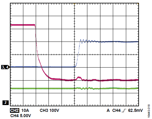
| Test | VDC (V) | fsw (kHz) | Duty Cycle (%) | IOUT1 (A) | VOUT2 (V) | POUT3 (W) | IIN4 (A) | Figures |
| 4 | 200 | 50 | 25 | 2 | 48 | 96 | 0.59 | Figure 16 and Figure 17 |
| 5 | 200 | 50 | 25 | 10 | 46 | 460 | 2.39 | Figure 18 and Figure 19 |
| 6 | 200 | 50 | 25 | 13.3 | 45 | 600 | 3.16 | Figure 20 and Figure 21 |
| 7 | 600 | 50 | 25 | 10 | 140 | 1400 | 2.42 | Figure 22 and Figure 23 |
| 8 | 900 | 50 | 25 | 10 | 204 | 2040 | 2.43 | Figure 24 and Figure 25 |
| 9 | 900 | 100 | 25 | 10 | 188 | 1880 | 2.52 | Figure 26 and Figure 27 |
|
1 IOUT is the output current in Load Resistor R1. 2 VOUT is the output voltage across R1. 3 POUT is the output power (IOUT × VOUT). 4 IIN is the input current through U1. |
||||||||


Schematic

Conclusion
The ADuM4135 gate driver has the current drive capability, the correct power supply range (30 V maximum), and a strong CMTI capability of 100 kV/µs to deliver good performance when driving SiC MOSFETs.
The test results provide data showing a solution is available on the market for isolated power supply, high voltage gate drivers driving SiC.
Author
