AN-1471: ADuCM4050 Flash EEPROM Emulation
Introduction
Nonvolatile data storage is a necessity in many embedded systems. Data, such as boot up configuration, calibration constants, and network related information, is normally stored on an electronically erasable programmable read only memory (EEPROM) device. The advantage of using the EEPROM to store this data is that a single byte on an EEPROM device can be rewritten or updated without affecting the contents in the other locations.
The ADuCM4050 is an ultra low power microcontroller unit (MCU) with integrated flash memory. The ADuCM4050 includes 512 kB of embedded flash memory with a 72-bit wide data bus that provides two 32-bits words of data and one corresponding 8-bit error correcting code (ECC) byte per access. The ECC is enabled by default for the user space on the ADuCM4050 and provides assurance that the flash initialization function works as expected. An ECC check is enabled for the entire user space in the flash memory of the ADuCM4050. If ECC errors are reported during any read operation, the ECC engine automatically corrects 1-bit errors and only reports on detection of 2-bit errors. When a read occurs on the flash, appropriate flags are set in the status register of the ADuCM4050. If interrupts are generated, the source address of the ECC error causing an interrupt is available in the FLCC0_ECC_ADDR register for the interrupt service routine (ISR) to read.
Emulation of the EEPROM on the integrated flash memory reduces the bill of material (BOM) cost by omitting the EEPROM in the design. The complexity of the code a user must write is reduced.
Background
Flash memory is typically organized as an array of pages. A single page in the ADuCM4050 is 2 kB. The contents of the page must be erased before writing data. The erase operation is universal to the page, whereas the read or write can be performed on a single addressable location (byte or word).
The challenges of performing the read or write on a single addressable location are as follows:
- Byte wide data read and write operations can be a challenge because the flash memory typically works at a block level for writing and erasing operations.
- The ability to erase or update data at any location while retaining data at other locations is difficult because flash memory erase operates on an entire page.
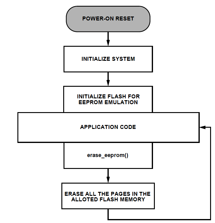
This application note describes the software using the ADuCM4050 device and the built in flash memory to emulate EEPROM, as shown in Figure 1.

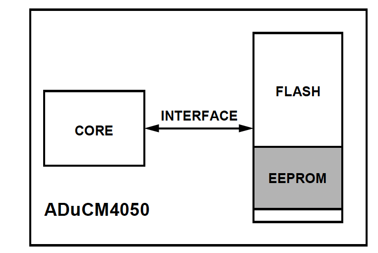
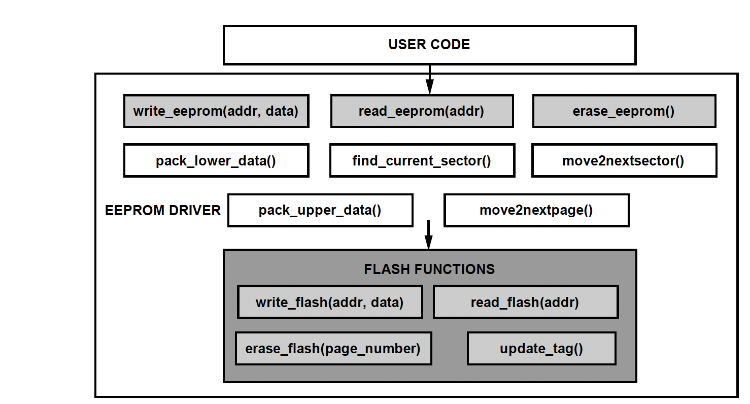
Figure 2 shows a block diagram of the EEPROM emulation code. High level functions provide the EEPROM emulation, whereas the low level functions implement the flash management and addresses conversion.

Working Principle
An EEPROM emulation requires a dedicated portion of the flash memory. Most EEPROMs can update one byte in one write command. Flash memory devices are equipped with multibyte writing capability and update the data accordingly, but only if erase sequences are followed between two write operations. To emulate a byte writable and readable EEPROM in the flash memory, it is necessary to follow a read, modify, and write sequence, which is similar to EEPROM operation.
The procedure presented in this application note uses two flash pages that can be extended to more than two pages, which are then divided into sectors consisting of sector tag. This sector tag provides information about the current sector under process and the number of data bytes written to that sector. The last location in each sector is reserved for the sector tag, which has a size that is equal to data bus size of the flash memory. The sector size and the number of sectors in a flash page depends on the size of the emulated EEPROM.
EEPROM
EEPROM writing and reading functions involve the processing of the application code input, such as EEPROM data and address information. The EEPROM application programming interface (API) handles processing and presenting the data and address information per the requirements of the flash interface.
Initialize EEPROM
The initialize EEPROM operation defines the size of the EEPROM and word length of the data in an EEPROM to be emulated. The maximum size of the emulated EEPROM is 2 kB (one flash page) because two flash pages are reserved for EEPROM emulation in this application software to maintain the data integrity. This limit can be increased if the same application software is extended from reserving two flash pages to four flash pages. Users can configure the word length from 8 bits to a maximum of 64 bits. See Table 1 for details regarding the init_eeprom(uint16_t eeprom_size, uint8_t word_length) function.
| Parameter | Description | Return Value |
| eeprom_size | Size of the EEPROM to be emulated. | No error. Write was successful. |
| word_length | Length of the data word to be written in the emulated EEPROM. Valid values are 8, 16, 32, or 64. | Error. The given address is out of the available EEPROM memory space. |
1 This function writes data to the EEPROM.
Write EEPROM
Figure 3 shows the EEPROM write operation flowchart. The EEPROM write operation procedure is as follows:
- Find the current sector by using the find_current_sector() function call. This search is based on the sector tag and the corresponding sector tag value. The value returned is the current sector start address, which is a physical location on the flash memory.
- Convert the EEPROM address to the flash address with the help of the current sector start address. Because the ADuCM4050 flash memory has a 64-bit wide data bus and the emulated EEPROM has an 8-bit wide data bus, the software determines the number of shifts required using the EEPROM address.
- Read the data at the obtained flash address. If the data is equal to 0xFF, the data to be written is first packed into two 32-bit data (pack_lower_data () and pack_upper_data()), and a 64-bit wide data is prepared to be written to the flash memory.
- Execute a write command on the flash controller by calling the write_flash() function. The input parameters for this function are the flash memory address and the packaged, 64-bit wide data.
- After a successful write operation to the flash memory, the sector tag of the current sector is updated by calling the update_tag() function.

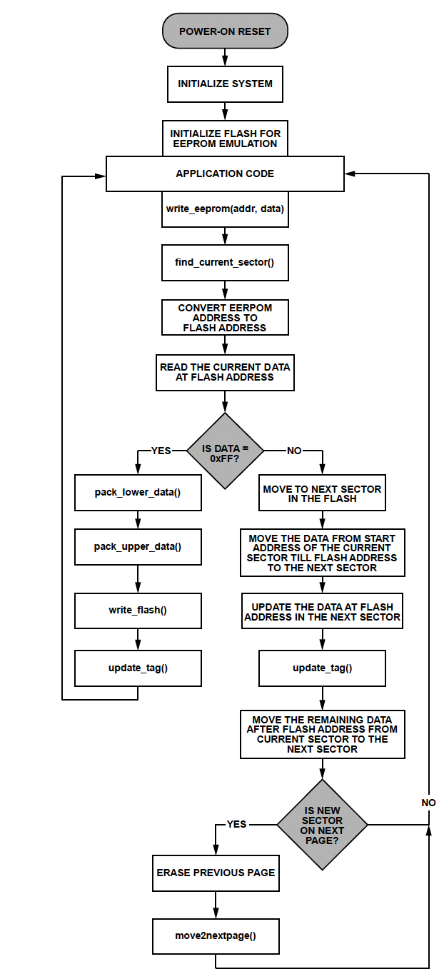
If data is already present at the obtained flash address, the data read function does not return 0xFF. In this case, the data before and after the obtained flash address is moved to the next or adjacent sector by calling the move2nextsector() function. The EEPROM data, which is converted to LSB and MSB data packets, is written at a new flash address in the next sector. Every time a write issues at an already written location of the EEPROM, the data moves to the next sector with the location in the next sector containing the modified data.
If the new sector resides on the next page, a flash page erase command is issued by calling erase_flash(page_number) to the previous page after the data is moved. All the address registers are updated by the move2nextpage() function.
See Table 2 for details regarding the write_eeprom(uint16_t addr_eeprom, uint8_t data_eeprom) function.
| Parameter | Description | Return Value |
| addr_eeprom | Logical address in the EEPROM space where data is to be written | No error. Write was successful.. |
| data_eeprom | Data to be written to the EEPROM space, pointed by addr_eeprom | Error. The given address is out of the available EEPROM memory space. |
1 This function writes data to the EEPROM.
Read EEPROM
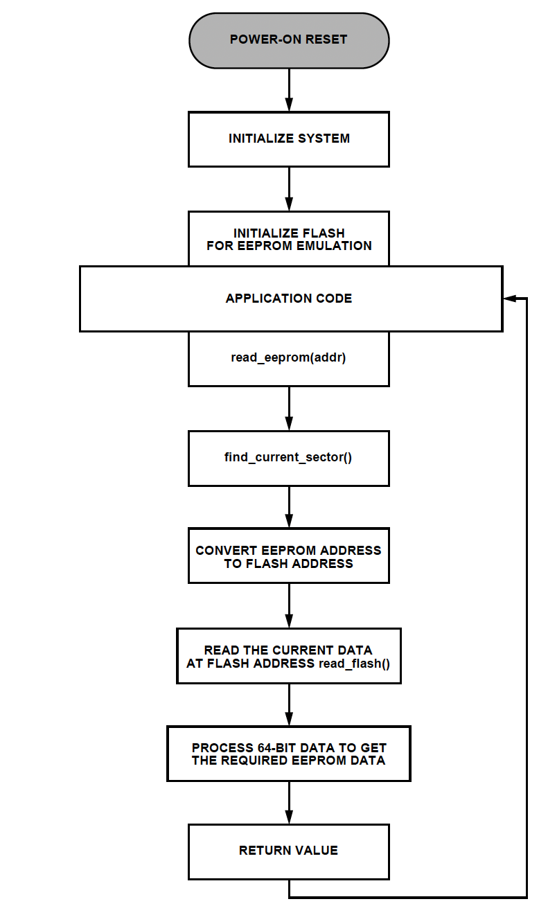
Figure 4 shows the EEPROM read operation flowchart. The EEPROM read operation procedure is as follows:
- Read the EEPROM value stored at the address location by calling the read_eerprom(addr) function.
- In an EEPROM read request from the application code, the software first determines the current sector, which consists of the latest data. A flash address is obtained using the EEPROM address and current sector start address.
- Execute a read command by calling the read_flash() function with the obtained flash address.
- Process the 64-bit wide data received from the flash address. The bits of this address are then masked, right shifted, and returned to the application code.

See Table 3 for details regarding the read_eeprom(uint16_t addr_eeprom) function.
| Parameter | Description | Return Value |
| addr_eeprom | Logical address in the EEPROM space where data is to be read | Value. The 8-bit data is returned to the application code. Error. The given address is out of available EEPROM memory space. |
1 This function writes data to the EEPROM.
Erase EEPROM
Figure 5 shows the EEPROM erase operation flowchart. The EEPROM erase operation procedure is as follows:
- Erase the entire EEPROM space allotted in the flash memory by calling the erase_eeprom() function.

All the pages in the flash memory dedicated to EEPROM emulation are erased. Use caution while using this operation in the application code.
See Table 4 for details regarding the erase_eeprom() function.
| Parameter | Description | Return Value |
| Not applicable | This function erases all the flash pages allotted to EEPROM | No error. Erase was
successful. Error. The flash controller is busy and cannot perform the erase action. |
1 This function erases the EEPROM memory space. All the data is lost if this function is called.
Flash
The ADuCM4050 processor includes 512 kB of embedded flash memory, available for access through the flash controller. The embedded flash memory has a 72-bit wide data bus, providing two 32-bit words of data and one corresponding 8-bit ECC byte per access. The memory is organized in pages of 2 kB each, plus 256 bytes reserved for the ECC. ECC is by default enabled on the entire user space of flash in the ADuCM4050. A write to a location of flash updates the data as well as ECC byte on that location. Because flash memory cannot change its bit value from Logic 0 to Logic 1 without an erase procedure, only one write operation is allowed. Therefore, ECC bytes update only once. The next write to the same location without the erase procedure leads to ECC error generation.
Flash WriteThe flash memory operates by setting bits to 1 when erased and selectively clearing bits to 0 when writing or programming data. No write operation is capable of setting any bit to 1 from 0. For this reason, generalized write accesses must be prefixed by an erase operation.
A keyhole write is an indirect write operation in which the code, usually programmed by the user, programs memory mapped registers with target address and data values, then commands the flash controller to perform a write operation in the background. The flash controller supports write access to the flash memory only through keyhole writes. This constraint on write access enables the flash controller to guarantee that writes occur properly as atomic double word (64-bit) operations.
The LSB and MSB data packets, which are created using EEPROM data, are provided to keyhole data registers. After the assertion of a write command, the flash controller initiates a 64-bit dual word write to the given flash address. Word (32-bit), half word (16-bit), and byte (8-bit) writes on the flash memory are not supported by the ADuCM4050 flash memory.
See Table 5 for details regarding the write_flash(uint32_t addr,uint32_t lower_data, uint32_t upper_data) function.
| Parameter | Description | Return Value |
| addr | The address in the flash memory space allotted for the EEPROM emulation | No error. Write was successful.. |
| lower_data | The lower 32 bits of the double word | Error. The given address is out of the available EEPROM memory space. |
| upper_data | The highest 32 bits of the double word |
1 This function receives the translated EEPROM address and data from the write_eeprom() function and issues a write command to the flash controller.
Flash Read
Flash memory is available to be read only after an automatic initialization process. Reading the flash memory returns a 64-bit double word.
Flash address information is provided to the flash controller, which returns the read data. This data is further processed by the EEPROM interface to achieve the EEPROM value.
See Table 6 for details regarding the read_flash(uint32_t addr) function.
| Parameter | Description | Return Value |
| addr | The address in the flash memory space allotted for EEPROM emulation | Read data. The 64-bit data is returned for masking
and is sent as the return value to the read_eeprom() function. Error. The translated address is out of the allotted flash memory space. |
1 This function receives the translated EEPROM address from the read_ eeprom() function and issues a read command to the flash controller.
Flash Erase
When there is a page change during an EEPROM write, a page erase command is asserted on the previous page by calling the erase_flash(page) function. Before a page erase, data movement occurs as detailed in the Write EEPROM section.
See Table 7 for details regarding the erase_flash(uint8_t PAGE) function.
| Parameter | Description | Return Value |
| PAGEr | The page number of the allotted flash memory space | No error. Page wise erase was successful. Error. The given page value is out of the allotted flash memory space. |
1 This function performs a page wise erase in the allotted flash memory space.
Limitations
In traditional EEPROMs, if one location updates, only one erase cycle is counted, followed by a write operation to that particular address while the other locations remain unchanged.
In the emulated EEPROM described in this application note, updating one location causes movement of data from the current sector to the next sector, which consumes the EEPROM size number of write cycles. Every time a location updates, data is moved to next sector and, if that sector resides on the next page, a page erase occurs. Data movement involving several writes decreases the effective endurance of the flash memory.
There are two ways to overcome these limitations. The first is to use caution when selecting the EEPROM size for emulation. A small EEPROM size decreases the write cycles during data movement, which indirectly increases the endurance of the flash memory. Avoid unnecessary writes to the EEPROM. By doing so, the effective endurance increases. For example, the system must issue writes only during a power fail sequence. A random access memory (RAM) buffer can be used for storing the data during normal operations.
The software handles some of the unnecessary writes to the emulated EEPROM. For example, if the data to be written is 0xFF and the current data at that particular location is 0xFF, no write command is issued to the flash memory.
Conclusion
This application note matches the physical difference between the EEPROM and the flash memory using the ADuCM4050. This emulated EEPROM is similar to a traditional EEPROM that overcomes the problems related to the silicon area, input/ output bus resources, manufacturing costs, and BOM.
This application note provides the user with a large EEPROM size ranging from 8 B to 2 kB (one page) because this application software reserves two flash pages for EEPROM emulation. If the software is extended to four flash pages, the maximum EEPROM size is 4 kB with a configurable word length from 8 bits to 64 bits.
Because there is a trade-off between the size of the emulated EEPROM and the endurance of the flash memory, select the appropriate size to enhance the hardware efficiency. The software handles some of the unnecessary writes to the ADuCM4050 flash device, which effectively increases the endurance.