AN-1446: Dither Generation in the AD5767
Introduction
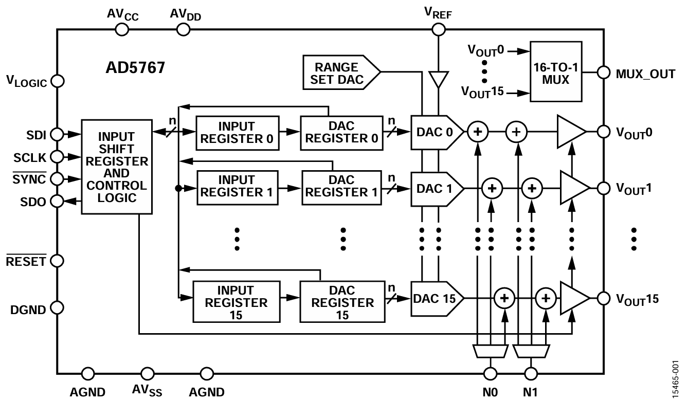
The AD5767 is a 16-channel, 12-bit, denseDAC® digital-to-analog converter (DAC) that can be configured to generate multiple output voltage spans from a minimum voltage of −20 V to a maximum voltage of +14 V from an external 2.5 V reference, while delivering up to 20 mA of output current per channel.
The AD5767 is recommended for biasing indium phosphide Mach Zehnder modulators (InP MZM), a common modulator used in optical communication.
The optimal dc bias point in the InP MZM changes due to physical stress or aging effects, for example. To find the optimum dc bias point and keep the modulator in perfect quadrature, a dither signal can be applied to the bias input voltage.
For this purpose, a feature has been integrated in the AD5767 that allows superimposing a low frequency, low voltage dither signal from 10 kHz to 100 kHz into the dc signal generated by the DAC, simplifying system design by reducing the bill of materials (BOM) and the printed circuit board (PCB) area.
The purpose of this application note is to discuss the different operation modes of the dither, as well as the optimum way to enable or disable this feature.
Figure 1 shows the block diagram of the AD5767.

Dither Specifics in the AD5767
How to Apply the Dither and Control Modes
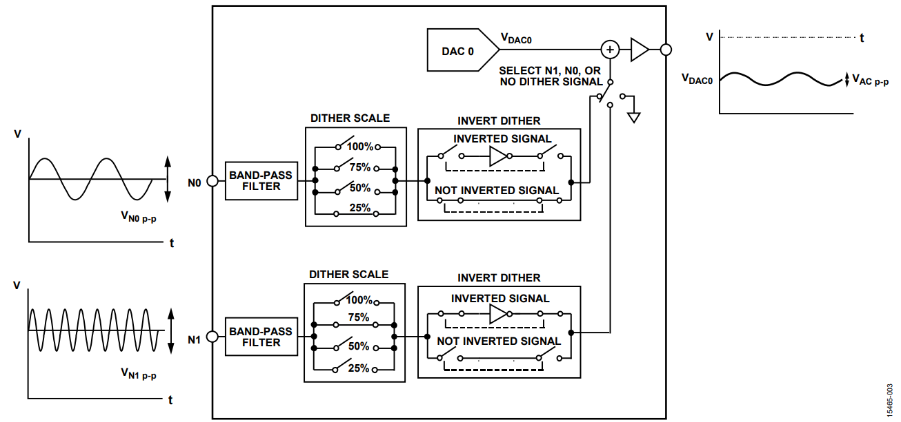
The AD5767 offers two independent input dither pins, Pin N0 and Pin N1, which are connected internally through multiplexers to the internal output buffer for each channel. The input dither pins can be disabled from all of the DAC output channels or enabled to any of the DAC channel outputs, while providing up to 20 mA of output current per channel. The dither input signal can be selected and applied to the DAC output channels by using Command x9 and Command xA.
Only one dither input signal can be applied to each DAC output channel at a time.
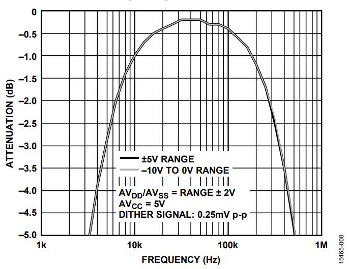
The N0 and N1 input dither signal pins are internally buffered to minimize the input current with an active band-pass filter (BPF) with a bandwidth of 90 kHz, from 10 kHz up to 100 kHz, as shown in Figure 8.
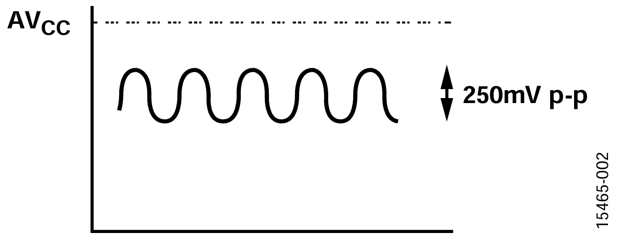
The maximum amplitude allowed for the dither signal is 250 mV p-p, with a maximum peak voltage of AVCC, as shown in Figure 2.

The AD5767 accepts any type of ac waveform as a dither input signal as long as the input frequency is within the bandwidth range of the BPF; otherwise, the filter adds additional distortion.
The dither input signal can be scaled and phase shifted individually for each channel before it is applied to the selected DAC output channel.
The amplitude of the dither signals can be scaled to 25%, 50%, 75%, or be left with its original amplitude by using Command xC or Command xD. The corresponding attenuation factor is selected per output channel.
The input dither signal phase can be inverted 180° by writing to the internal invert dither register using Command xB.
The gain, the phase, and the availability of the external dither signals can be modified at any time during operation.

Monitoring Dither
The AD5767 integrates a 16:1 internal multiplexer. This multiplexer allows the selection of any DAC output channel to be monitored through the MUX_OUT pin at any given time by writing to the internal monitor mux control register using Command x0.
To disable the multiplexer, clear the VOUT_SEL bits from the monitor mux control register.
The internal monitor mux is not internally buffered; consequently, it is recommended to use an external buffer to minimize the load effect at the selected monitored channel, because any external current on the MUX_OUT pin affects the DAC channel monitored.
DAC Output Effects
When the dither is enabled, a series of effects must be taken into consideration because some second-order effects can affect the output channels.
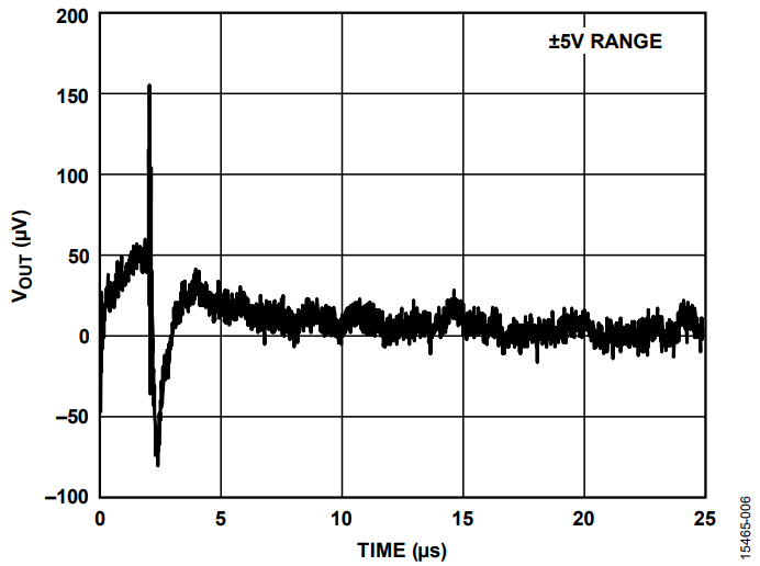
Dither Enable or Disable Energy Transients
A series of fast transients is seen in the selected DAC output channel when the dither is enabled or disabled in the selected channel due to the energy injected by the dither switches to the DAC output buffer.


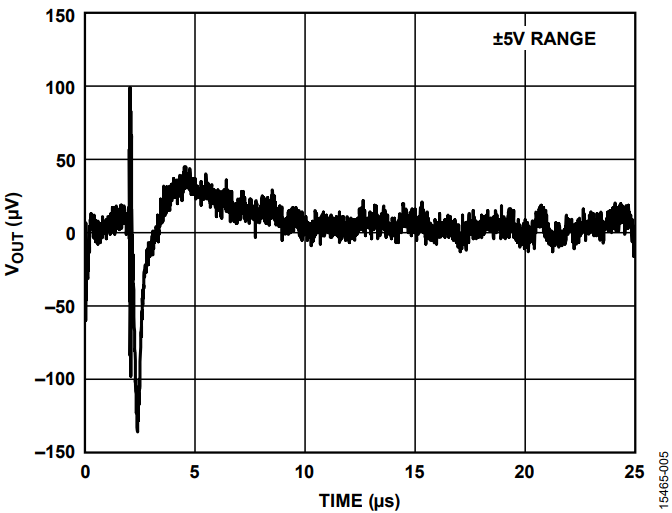
In addition, some fast transients can be observed in the nonselected DAC output due to coupling between internal digital lines, as shown in Figure 6.

For optimum performance, it is recommended to configure the dither inputs before the AD5767 output span is configured, because the outputs are clamped to AGND, and apply the dither signal after the voltage span is configured.
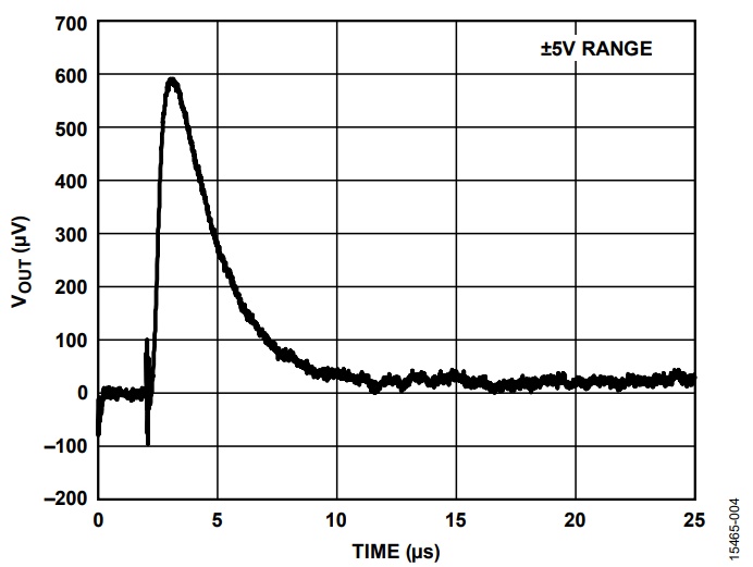
DC Shift
The addition of a dither tone signal to a DAC output channel increases the output voltage of this DAC slightly. This phenomenon is due to the current injected by the dither buffers to the DAC output buffer.
Figure 7 shows the effects of enabling the dither signal onto a DAC output voltage.

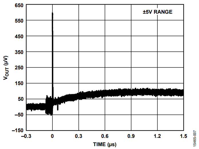
If the dither is enabled at power-up, the dc offset generated by the dither buffer can be computed as an increment of the offset error.
Amplitude Attenuation and Phase Shift
The dither input pins, Pin N0 and Pin N1, integrate an active band-pass filter to remove the dither dc voltage and prevent instability in the DAC output buffer. The lower cutoff frequency is 10 kHz, and the upper cutoff frequency is 100 kHz.
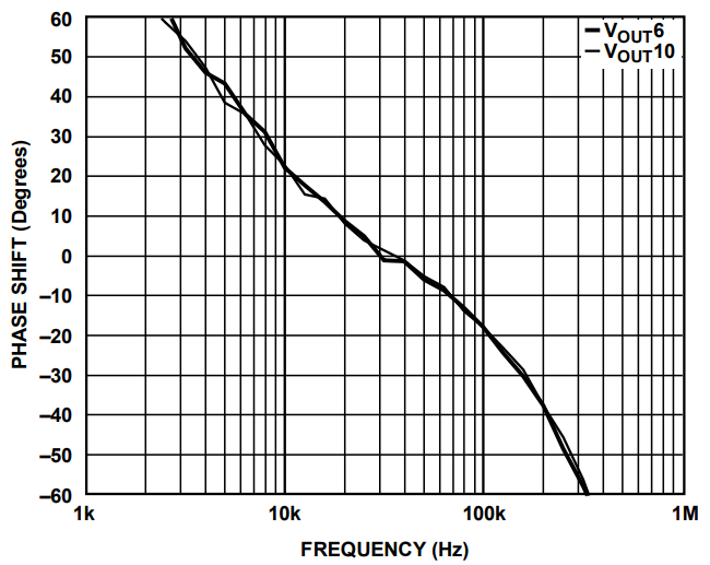
There is a certain dependency on the input dither transfer function with the selected output voltage range in terms of attenuation and phase shift. Figure 8 and Figure 9 show typical performance at the ±5 V output voltage range.


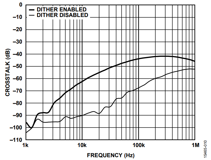
Crosstalk
When a dither tone is applied in one channel, crosstalk can be observed in the adjacent channels. The magnitude of crosstalk transferred to adjacent channels depends on a different dither tone signal or no dither tone signal being applied to these channels.

Total Harmonic Distortion (THD)
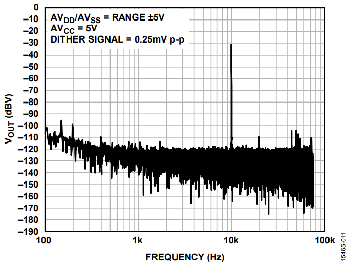
The total harmonic distortion for the input dither signal across the multiple internal buffersin the AD5767 is shown in Figure 11.

Best Practices to Obtain the Best Performance
To obtain the best performance from the DAC when using the dither capability while operating the AD5767, initially configure the dither before removing the output clamp to ground.
The recommended sequence to operate the AD5767 using the dither functionality minimizes the transient amplitude seen on the DAC outputs when the dither functionality is enabled or disabled.
The recommended configuration of the dither is as follows:
- When the AD5767 is powered up, configure the input dither signals by using Command x9, Command xA, Command xB, Command xC, and Command xD.
- Configure the AD5767 for normal operating mode before applying the dither signal to the input pins. To configure the AD5767 for normal operating mode, the span register must be configured to allow the output clamp on the AD5767 to be removed by using Command x4.
- To finalize the dither configuration, apply the N0 and/or N1 input dither signals.
When applying the dither signals to the DAC outputs before the span register is configured, expect an injection of transients on the DAC outputs. Limiting the dc component of the dither signals to 1 V helps to reduce the amplitude of the transients; however, it must be noted that this mode of operation is not recommended.
Authors

