AN-1444: Second-Order Effects to Consider for Continuous Precision DAC Updates
AN-1444: Second-Order Effects to Consider for Continuous Precision DAC Updates
Introduction
As opposed to precision analog-to-digital converters (ADCs) that have clearly defined and characterized number of samples per second, precision digital-to-analog converters (DACs) do not have this defined in data sheets because it depends on many factors.
In most cases, the DAC digital interface allows clock rates up to 50 MHz, which, assuming a 24-bit input shift register, equates to a potential 2,000,000 writes per second. However, this number only represents the capabilities of the digital interface to accept a new DAC code without accounting for the digital process delay, latency, and analog block timing.
The latency becomes negligible if the DAC does not include any internal calibration procedure, typically in the range of a few nanoseconds. If the DAC includes a calibration routine, the latency can be in the range of 1 μs to 3 μs.
From the analog block, there are two different case scenarios related to a new code update:
- The update speed is limited by the bandwidth of the active stage connected to the DAC, typically a buffer, which can be internal or external.
- The update speed is not limited by the active stage, but by the DAC core.
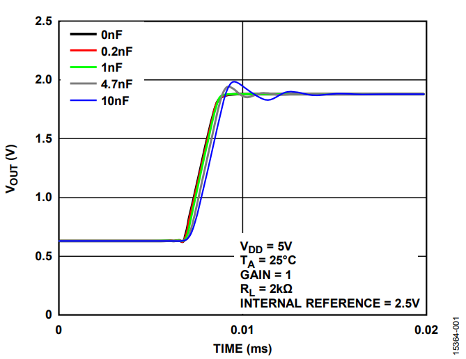
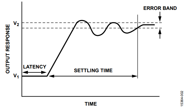
In the first case, the settling time specification provides a good estimate of the capabilities of the analog block. The settling time is defined against the new code related to the previous one, usually from ¼ to ¾ scale, within a defined tolerance that is approximately one least significant bit (LSB) around final code.
For a large step code transition, the slew rate is the major contributor in the settling time. Additionally, the settling time can be increased due to the imaginary component in the output load, similar to capacitors or inductors, generating an overshoot or ringing.
The value of the imaginary impedance connected externally dictates the overshoot magnitude, affecting the settling time, as shown in Figure 1.

The final settling time is the contribution of latency, slew rate, and ringing times, as shown in Figure 2.

The smaller the code step required and the lower the capacitance connected, the faster the final settling time.
When the new code is near the previous code, the settling time or buffer capabilities are not limiting; this can be considered a fine tune update.
In this case, the latency and dynamic effects of the DAC core are the dominant factors that limit the time the output takes to become settled within the defined tolerance range, that is, 1 LSB around the final code.
The dynamic effects are generated when the DAC is operated, as some of the energy generated internally from the digital block (to shift in the data from external pins or processing the command) and the analog block (to update the output to the new code) transfer externally. In particular, the main two specifications are digital feedthrough and digital-to-analog glitch energy.
In the case of a coarse tune of the output, some of this energy is hidden by the slew rate of the buffer, as this is the main contributor injecting energy to the output load, whereas in the case of a fine tune update, both specifications are visible and measurable.
DAC Core Dynamic Effects
Any DAC operation generates internal peaks of current or voltage that must dissipate through the supply pins, typically VDD or GND. Due to internal parasitics, the energy generated internally when the DAC is operated cannot be completely dissipated through these paths, and a portion of this energy is transferred to the output load, affecting the output stability.
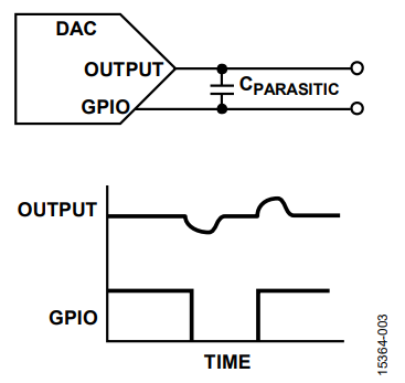
The digital feedthrough is the phenomenon when transition on an external digital pin generates a disturbance on the internal DAC during the transition commutation.
Additionally, the digital feedthrough can be amplified externally by an incorrect printed circuit board (PCB) layout.
Best PCB layout practices include keeping the digital lines in the PCB away from the PCB analog lines, or at least avoiding analog traces running in parallel to digital traces to minimize the external coupling effects. Figure 3 shows an example of digital feedthrough caused by an incorrect layout.

The digital feedthrough is a typical specification because the energy transfer to the load depends on multiple factors, such as digital input levels, slew rates, and the number of digital lines toggled (data transmitted).
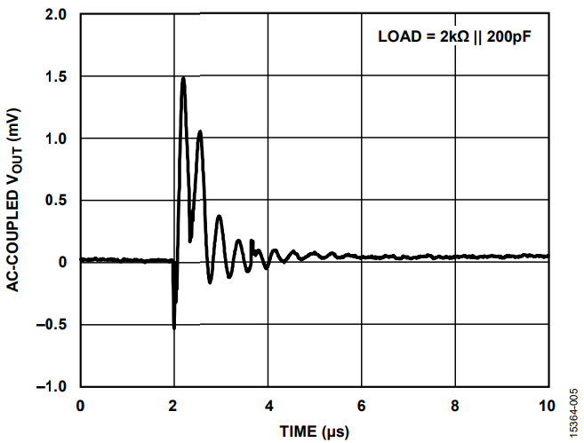
The specification measures the area (nV-s) of the energy transferred externally. An example of the effect of the digital feedthrough associated with a write to the input register is shown in Figure 4.

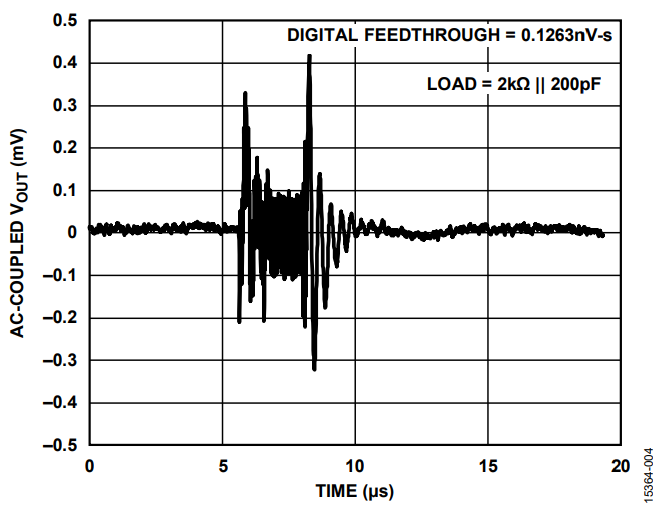
The energy associated with the digital feedthrough is measured by writing a command to the DAC to not update the DAC core output (such as updating the control register) to avoid measuring other effects that can potentially increase the energy generated internally (that is, the energy generated when the DAC core is updated) or the extra energy associated with any internal calibration routine.
The energy generated during any internal calibration routine is included in the digital-to-analog glitch. The digital feedthrough is present in each write/read access.
When the DAC core output is updated, another dynamic phenomenon can be observed on the DAC output in the form of a glitch. This specification is related to the different propagation delays between internal switch control lines in the DAC core, referred to as digital-to-analog glitch impulse, or glitch energy, because it is generated when the digital word is converted to analog by toggling the switches to select DAC resistors.
The digital-to-analog glitch impulse is inherent to the device but worsens by improper PCB layout in the same manner as digital feedthrough.
The digital-to-analog glitch impulse typical performance is also measured in terms of net area (nV-s) as 1 LSB transition around the major carry transition; for a 16-bit DAC, the major carry is toggling between DAC code 0x7FFF and code 0x8000, which typically requires most of the DAC switches to change.
Figure 5 shows an example of the effect of the digital-to-analog glitch impulse associated with a write to the DAC register. To disregard the digital feedthrough contribution, the DAC updates using a delayed hardware LDAC event, after the energy generated by the digital feedthrough completely dissipates.

Different DAC codes generate different glitch energy because different switches are involved in the change of code.
The worst case for the digital-to-analog glitch is not always the major code transition, 1 LSB around midscale code. This depends on two factors: the internal parasitic in the layout and the internal parasitic in the DAC (including an internal calibration engine). Physically, the digital midscale code is not always midscale DAC code. However, the digital major code transition is assumed as a good reference to quantify the digital-to-analog glitch energy.
Propagation of DAC Core Dynamic Effects
Whereas the slew rate and output ringing at the output are events at low frequency, digital feedthrough and digital-toanalog glitch impulse are predominantly medium to high frequency effects.
Digital feedthrough is generated at frequencies related to digital transmission, such as the 50 MHz clock speed, or even higher speeds. For example, with a slew rate of 1 nV/s, the tones can be as high as 300 MHz. Figure 4 and Figure 5 show the fast transients that can be observed due to the frequency of the dynamic events.
In all cases, some of the energy generated internally can be measured externally, as shown in previous plots. The dynamic energy transferred to the load depends on the external capacitor connected to the output pin, which generates an increment of voltage defined by
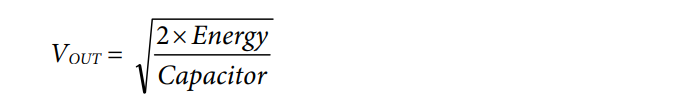
where:
Capacitor is the external capacitor value.
Energy is the energy transferred externally through the dynamic
events.
From bench measurements, the increment of voltage is relatively independent of the capacitor connected externally because the dynamic energy transferred externally dissipates through the DAC output pin, providing a low impedance path.
Continuous DAC Operations
If the DAC is continuously updated in applications that require a fast fine tune, the energy transferred to the load does not completely dissipate, consequently measuring an extra offset at the output.
The value of the voltage increment depends on two factors, the value of the energy transferred, and the time that the capacitor has to discharge, as shown in Figure 6.

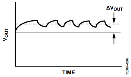
It is assumed that the DAC is continuously updated and, consequently, the energy generated internally is the contribution of both digital feedthrough and analog glitch.
In some cases, the increment of voltage is only due to the digital feedthrough contribution when the DAC access is to the read/ write register only and no DAC core update action is performed.
AD5686R 4-Channel, 16-BIT nanoDAC+ Case Study
To illustrate these concepts, the AD5686R is used as an example case.
Updating the AD5686R output continuously delays the time between writes, from 1 μs to 20 μs.
The energy generated internally is transferred during an approximate 1 μs period, which is the sum of the digital feedthrough duration, 24 bits at 36 MHz SCLK clock, and the duration of the analog glitch.
When the update time is similar or longer than the energy event, depending on the capacitor value, shown in Figure 7, the increment of voltage generated can be approximated as
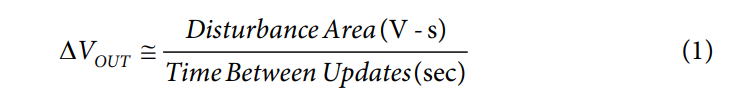

At a 1 µs update, the increment of the voltage measured matches the digital feedthrough energy and the analog glitch, 0.13 nV-s + 0.5 nV-s = 0.63 nV-s, as shown in Figure 8.

As an example, if the disturbance is 0.63 nV-s, and the update frequency is 2 µs, the increment of voltage generated is
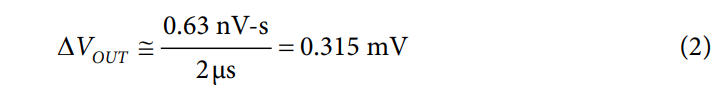
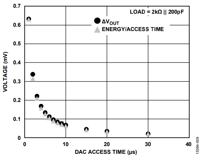
Figure 9 shows the correlation between the bench measurements and Equation 1.

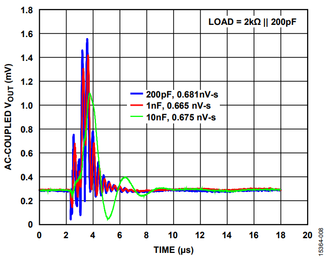
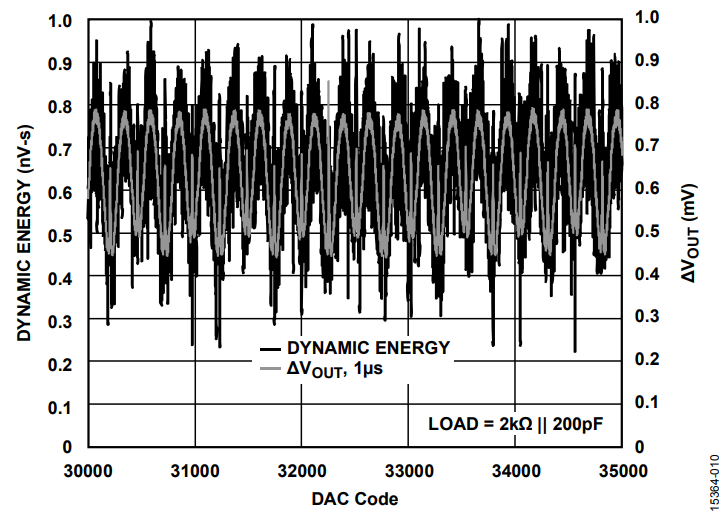
Not all codes result in the same net area and show a slightly different ΔVOUT. A sample of results for codes around midscale is shown in Figure 10. Codes resulting in higher dynamic energy also demonstrate higher ΔVOUT. The average energy is commensurate with the AD5686R data sheet specifications (~0.6 nV-s).

To measure dynamic energy with good resolution, the output signal must be ac-coupled. Thus, when trying to measure dynamic energy with high access time, a portion of the dc component can be lost. Consequently, the ΔVOUT (dc value) is a better way of quantifying this excess energy that does not have enough time to dissipate when the DAC access time is too fast.
As previously mentioned, the net area measured is independent of the capacitor that is connected externally, as shown in Figure 7.
In Table 1, the ΔVOUT measurements for a given access time and different load capacitances show small differences.
| COUT | Access Time | ||
| 1 µs | 5 µs | 10 µs | |
| 200 pF | 631 μV | 133 μV | 67 μV |
| 1 µF | 661 μV | 134 μV | 67 μV |
| 10 µF | 622 μV | 130 μV | 66 μV |
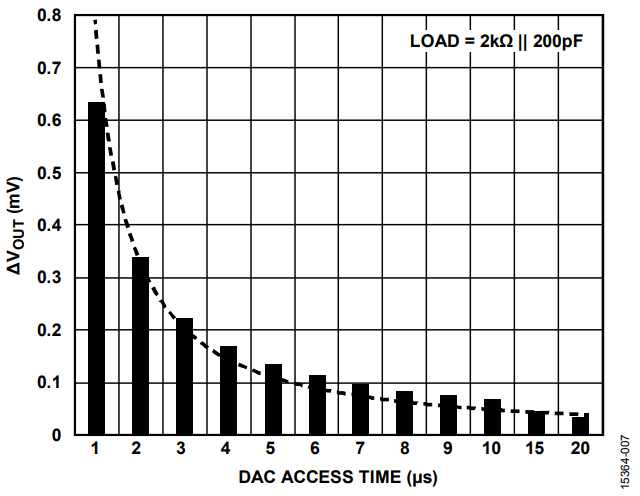
Table 2 presents the measured ΔVOUT for the AD5686R at different DAC access times. The typical ΔVOUT due to both digital feedthrough and digital-to-analog glitch impulse is reported for different access times when the DAC output is updated, together with results for digital feedthrough only, when the DAC code is written to the input register but not updated at the output.
| DAC Access Time (μs) | ΔVOUT Feedthrough and Glitch (μV) | ΔVOUT Feedthrough Only (μV) |
| 1 | 618 | 210 |
| 2.5 | 320 | 110 |
| 5 | 215 | 72 |
| 10 | 150 | 54 |
| 20 | 120 | 43 |
Conclusion
Because of the nature of these dynamic phenomena and their effect being so dependent on parasitics and coupling mechanisms, they can differ from DAC to DAC. The dynamic effects of the phenomena impact changes depending on the specific application, the circuit configuration and operating conditions.
For coarse updates of the DAC output the settling time and latency are the limiting in terms of DAC update rate. When only a fine tune of the DAC output is involved, or when writing to the device without updating the output, the excess energy generated by the DAC core dynamic effects can generate some extra offset.
If the dc performance is critical in the application, do not operate the DAC at its fastest access time (as determined by the digital interface). When the application specifically requires faster update rates, the energy area must be assessed to understand its potential impact to system performance. To quantify this impact properly, the best approach is to rely on actual measurements. When the excess of dc voltage (ΔVOUT) is present in the system, it is advisable to measure it for different access times, removing the need for complicated and less reliable ac measurements.
In general, when working with DACs, define a reliable access time (update rate) that carefully assesses both the dynamic performance (settling time, digital feedthrough, and digital-to-analog glitch) and the system configuration.
Authors

