Introduction
Part 1 of this article discussed the history of the Wien bridge oscillator and its theory of operation, while exploring simulations with idealized circuit elements. In Part 2, we will analyze and construct a practical Wien bridge oscillator and then measure its performance. As an added bonus, we will build and test an alternate circuit with considerably better performance.
Design files for a printed circuit board (PCB) are available so you can build one of your own as you read along.
Simulation and Construction of a Complete, Practical Wien Bridge Oscillator
We’ve informally discussed using a light bulb as a gain control element. While this does work, you can’t choose just any light bulb and expect the circuit to operate properly, the bulb must be chosen carefully. Let’s first explore a practical implementation using antiparallel diodes to gently control the amplifier’s gain.
Materials
- ADALM2000 (M2K) Active Learning Module OR:
- Two-channel oscilloscope, signal generator, and/or network analyzer functionality
- ±5 V bipolar tracking power supply
- ADALP2000 parts kit items:
- Solderless breadboard
- Jumper wire kit
- Two 10 nF capacitors
- Two 1 μF capacitors
- Three 10 kΩ resistors
- Two 4.7 kΩ resistors
- One 5 kΩ single-turn potentiometer
- Two 1N4148 silicon diodes
Alternatively, PCB files with matching LTspice® simulations are available to fabricate a PCB for this experiment, which are available as Wien Bridge PCB files and LTspice files.
The circuit shown in Figure 1 is a complete (and practical) Wien bridge oscillator circuit that can be built on a breadboard. Rather than using an incandescent bulb (with effective resistance that increases with applied voltage) for the amplifier’s input resistor, this circuit shunts part of the feedback resistance with diodes, whose effective resistance drops with applied voltage. Ignoring the diodes, the gain would be 1 + (10k + 4.7k)/(4.7k + 2k), or about 3.19 (recall that an ideal Wien bridge requires a gain of 3.0 to sustain oscillation). But as the voltage across D1 and D2 approaches 600 mV or so, the resistance of the parallel combination of D1, D2, and R2 is reduced, dropping the gain.


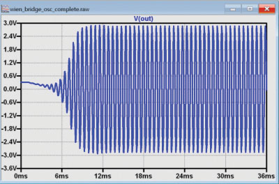
Open wien_bridge_osc_complete.asc in LTspice and run the simulation; the output should resemble the simulation in Figure 2. The V3 kick circuit applies a 0.1 V, 5 ms pulse to the bridge immediately after the simulation begins. While this circuit isn’t strictly necessary for the simulation to start, it does help the simulation reach steady state much faster. Without the kick, the simulation would still start eventually, but the amplifier’s low offset in the model can cause a significant delay. Startup time is also a concern in some real-world applications, and circuits similar to V3, such as a pulse generator made from logic gates, can be employed. Experiment with different values for vkick (including zero).

Next, construct the circuit as shown in Figure 3.


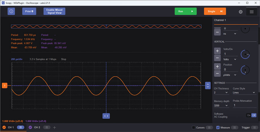
Note that R5 is a potentiometer, allowing the gain of the circuit to be dialed in to where oscillation just starts. Measure the output with Scopy’s oscilloscope; set the vertical to 1 V/div and the timebase to 200 μs/div. The results should be similar to Figure 4.

That is a nice looking sine wave, but how nice is it? Can your eye detect any distortion at all? It is nearly impossible to visually detect distortion in a time-domain (oscilloscope) plot—even with a perfect reference sine wave to compare against, distortion less than 1% is difficult to see. To truly analyze low level distortion components, Fourier transform techniques are required, and that is exactly what Scopy’s spectrum analyzer does. Open the spectrum analyzer, and set the Start frequency to 0 kHz, Stop frequency to 20 kHz, Top to 0 dB, and Bottom to –120 dB. IMPORTANT: Click the Channel 1 settings, select Blackman-Harris window, and set the Gain Mode to High.
Note:
The ADALM2000 has two input ranges, ±2.5 V and ±25 V. These are selected automatically in the oscilloscope as you adjust the vertical gain, but not in the spectrum analyzer. If you increase the oscillator’s gain to the point where the output exceeds ±2.5 V, you will need to set the Gain Mode to Low to avoid clipping, which will not damage anything but will result in excessive distortion.
Observe the spectrum of the oscillator’s output, as in Figure 5.

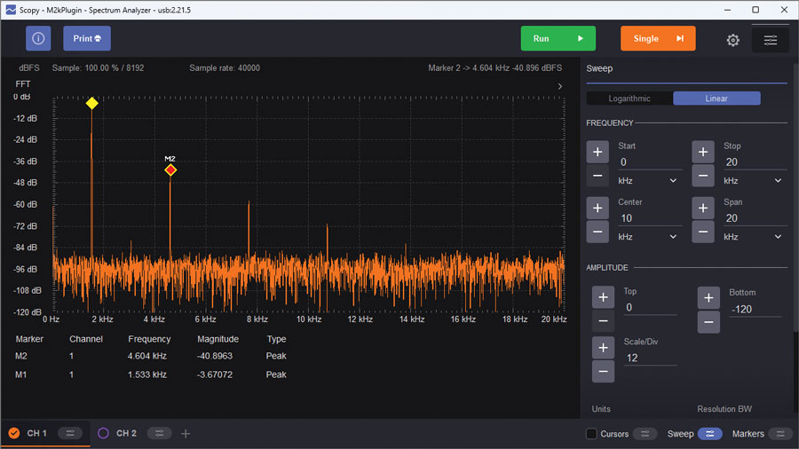
While the diode clamp method of limiting the gain is simple, it’s difficult to get better than approximately –40 dB (about 1%) distortion.
Questions
1. What is the relationship between the gain control elements and distortion?
2. What would happen to the distortion components (harmonics) if you replaced one of the diodes in the diode clamp circuit with a Schottky diode, which has a lower forward drop than a silicon diode?
A Much Lower Distortion Version of the Circuit
Let’s build up a variant of the circuit shown in Figure 1 of Part 1 of this series. The #327 incandescent bulb is a 28 V indicator lamp with a cold resistance of approximately 130 Ω and a hot resistance of approximately 650 Ω. This can be modeled as a resistor in LTspice, with resistance being a function of the power dissipation. But the resistance can’t change instantaneously—if it did, then as the output sine wave went from zero, to full-amplitude, back to zero, and to full negative amplitude, the amplifier’s gain would change in concert, distorting the output waveform; this is NOT what we are after.
The operation of the circuit relies on the bulb’s thermal time constant being much longer than half the output period. Why half the output period? Recall that the formula for power dissipated in a resistor is V2/r, so both positive and negative output swings produce positive power dissipation. This time lag is modeled by translating the bulb’s power dissipation into a current, which drives a parallel R-C network (R100 and C100), with a resulting time constant of 50 ms—much longer than the 628 μs half-period of the 1.59 kHz output. Thus, the bulb’s resistance is dependent on the average power dissipation over many cycles.
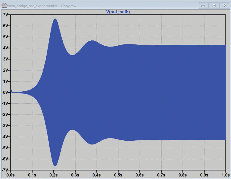
Open the wien_bridge_osc_experimenter.asc simulation, shown in Figure 6. Note that this simulation file is in the PCB design files folder.


Run the simulation and probe the output, as shown in Figure 7.

Note the initial transient, where the circuit is searching for just the right amplitude to sustain oscillation. While this circuit may be built up on a breadboard, if you have made it this far into the exercise, you might want to have something a bit more reliable and permanent. Figure 8 shows the completed PCB with the ADALM2000 connected.

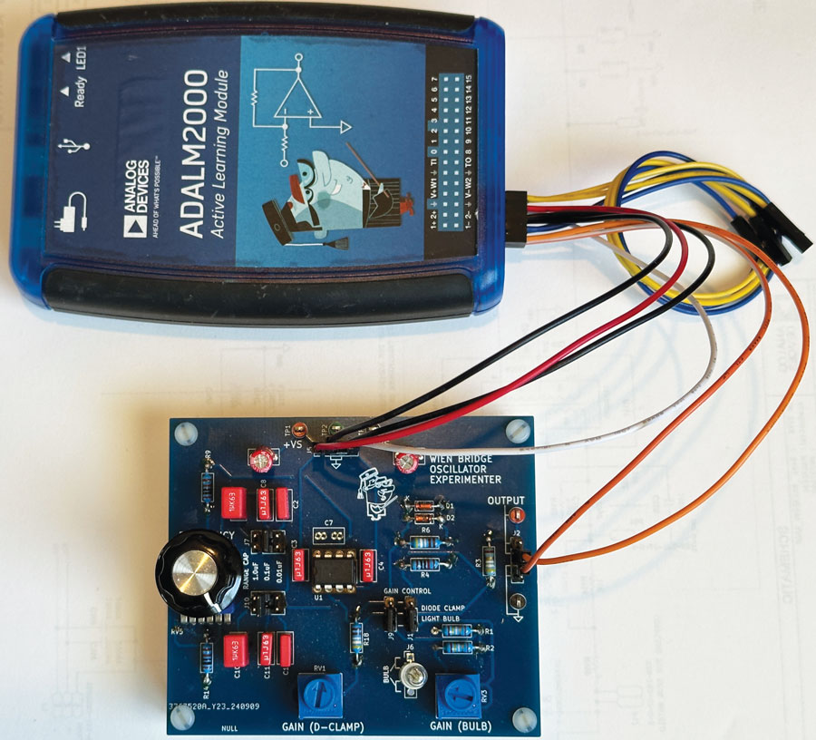
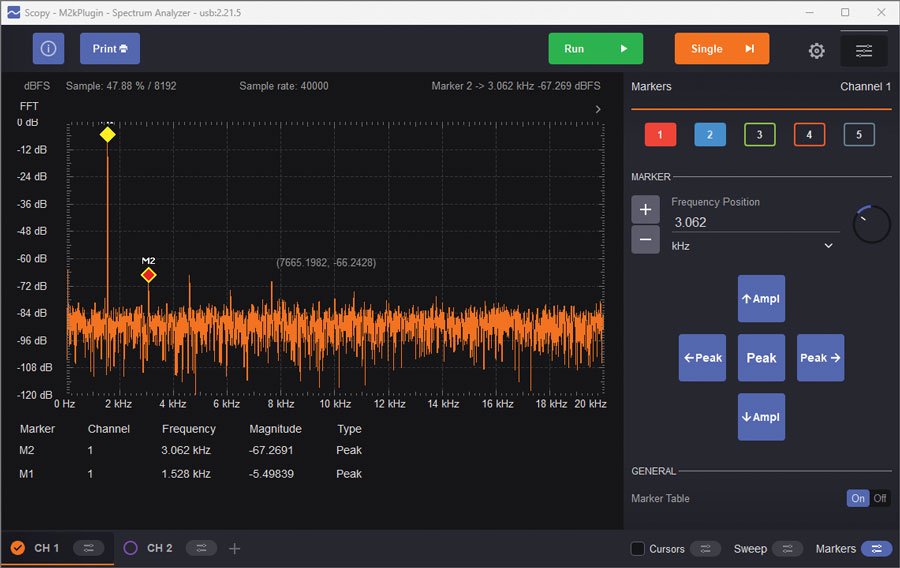
Figure 9 shows the output spectrum of the Wien bridge oscillator experimenter board set to bulb control. Note that the third harmonic is better than –60 dB, or 0.01%—10 times lower than typically achievable with the diode-clamp circuit. In fact, this is pushing the distortion floor of the ADALM2000 itself! While the exact number varies, there’s an axiom that a measurement instrument should be 4 to 10 times better than the device under test. We have reached the limit of the ADALM2000; the only option for confidently measuring this circuit’s distortion is to use a better test instrument.

Conclusion
While Part 1 focuses on the background and theory of the Wien bridge oscillator, Part 2 provides a detailed exploration of practical implementations with an exercise to build your own to enhance your understanding. Now you have a high performance oscillator whose operation you thoroughly understand. What to do with it now? It’s a perfect excuse to repurpose an old cookie tin as an enclosure—find some funky knobs and a junk box power switch and you’ve got a unique piece of test equipment to wow your friends, family, and coworkers.
Questions
3. What is the state of the art for distortion measurement instruments in the audio range?
4. If you can’t afford a state of the art benchtop distortion analyzer, are there other options? (Hint: Watch the video in Part 1 of this series!)
You can find the answers at the StudentZone blog.
References
Hewlett, Bill. “A New Type Resistance-Capacity Oscillator” (master’s thesis). kennethkuhn.com, May 2020.
U.S. Patent 2,268,872: Variable Frequency Oscillation Generator.
“Using Lamps for Stabilizing Oscillators.” Tronola, October 2011.
Wien Bridge Oscillator. Wikipedia.
Williams, Jim “Application Note 43: Bridge Circuits—Marrying Gain and Balance.” Linear Technology, June 1990.
Williams, Jim. “Thank You, Bill Hewlett.” EDN Magazine, February 2001.
Williams, Jim and Guy Hoover. “Application Note 132: Fidelity Testing for A-D Converters.” Linear Technology, February 2011.
Acknowledgements
This exercise was inspired by an ASEE 2022 conference workshop presented in partnership with Dr. Robert Bowman, author of the book EE Freshman Practicum. The full workshop video is available on YouTube.
