Objective
In circuit design, it is important to consider the wide variation in certain device values from one to another. A central objective of the designer is to desensitize the circuit to these variations in order to produce a circuit that meets the specifications across all possible conditions. One aspect of design that is common to nearly all circuits is the establishment of stable bias or operating point levels. This seemingly minor portion of the design can provide the most challenging and interesting circuit problems. Many bias generators are centered around the generation of currents to operate the core of the circuit. Current generated from simple resistors and diodes or diode-connected transistors connected across the power supply will vary approximately proportional to the variation of the supply voltage. This variation in the resulting bias current is frequently undesirable.
This is to introduce a current mirror, examined in previous activities, which has an output that has been desensitized to variation in input current. To understand those circuits, it is helpful to examine the behavior of a zero-gain amplifier.
Materials
- ADALM2000 Active Learning
- Solderless breadboard
- One 2.2 kΩ resistor (or any similar value)
- One 47 Ω resistor
- One small signal NPN transistor (2N3904 or SSM2212)
Directions
In Figure 1, we have a transistor biased into conduction with a collector voltage that is less than the base voltage by kT/q (equal to IC times 47 Ω) and is essentially constant with input voltage changes applied from the AWG generator.

Hardware Setup
The breadboard connections are shown in Figure 2. The waveform generator W1 output drives one end of resistor R1. Resistor R2 is connected between the base and collector of transistor Q1 with the other end of resistor R1 connected to the base as well. The emitter of Q1 is grounded.

Procedure
The waveform generator 1 should be configured for a 1 kHz triangle wave with 3 V amplitude peak-to-peak and 1.5 V offset. Connect Scope Channel 1 to display output W1 of the AWG generator. The single-ended input of Scope Channel 2 (2+) is used to measure alternately the base and collector voltage of Q1.
Configure the oscilloscope instrument to capture several periods of the two signals measured. Make sure to enable the XY feature.
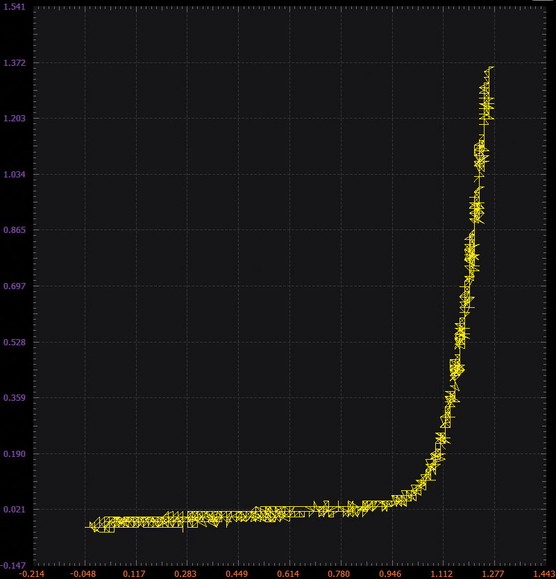
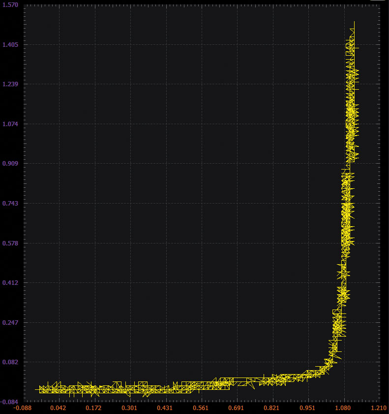
Plot examples using the oscilloscope are provided in Figure 3 through Figure 5.


Improved VBE Multiplier, Applying the Zero-Gain Concept
Many circuits require the generation of a voltage greater than 1 VBE. Here we explore in more detail three additional ways to accomplish this.
VBE Times 2 Version 1:
The obviously simple thing to do would be to just use two diode-connected transistors in series.
Materials:
- One 1 kΩ resistor
- Two small signal NPN transistors (2N3904 or SSM2212)
Directions:
The breadboard connections are shown in Figure 7. The output of the AWG generator drives one end of resistor R1 as well as the 2+ input of Scope Channel 2. The emitter of Q1 is connected to ground. The base and collector of Q1 are connected to the emitter of Q2. The base and collector of Q2 are connected to the other end of R1 and to the 2– input of Scope Channel 2 and the 1+ input of Scope Channel 1.

Hardware Setup:
The waveform generator should be configured for a 1 kHz triangle wave with 3 V amplitude peak-to-peak and 1.5 V offset. Both scope channels can be set to 200 mV per division.
Procedure:
Configure the oscilloscope instrument to capture several periods of the two signals measured. Make sure to enable the XY feature.

For a plot example using the oscilloscope, see Figure 8.

VBE Times 2 Version 2:
A second option would be to use two resistors as a voltage divider. This could produce an output that is the addition of fractions of a VBE to the VBE of Q1.
Materials:
- One 1 kΩ resistor
- Two 10 kΩ resistors
- One 5 kΩ variable resistor (a 500 Ω potentiometer would be preferable if available)
- One small signal NPN transistor (2N3904 or SSM2212)
Directions:
The breadboard connections are shown in Figure 10. The output of the waveform generator drives one end of resistor R1 as well as the 2+ input of Scope Channel 2. The emitter of Q1 is connected to ground. Resistor R3 is connected between the base of Q1 and ground. One end of resistor R2 is connected to the other end of R1, to the 2– input of Scope Channel 2, and one end and the wiper of potentiometer R4 2–. The opposite end of R2 is connected to the base of Q1. The collector of Q2 is connected to the remaining end of R4 and the 1+ input of Scope Channel 1.

Hardware Setup:
The waveform generator should be configured for a 1 kHz triangle wave with 3 V amplitude peak-to-peak and 1.5 V offset. Both scope channels can be set to 200 mV per division.
Procedure:
Start out with variable resistor R4 set to its minimum value of nearly 0 Ω. Observe the voltage vs. current characteristics of this configuration compared to version 1. There is a small extra current that flows in the two 10 kΩ resistors before the transistor turns on. The voltage at 1 mA is slightly higher, and the slope of the curve is not as steep.
Configure the oscilloscope instrument to capture several periods of the two signals measured. Make sure to enable the XY feature.

Plot examples using the oscilloscope are provided in Figure 11 and Figure 12.

Let’s apply the concept of the zero-gain amplifier. Now adjust R4 and observe the slope of the curve change. At what value of R4 is the curve nearly vertical? Why is that value the correct value for zero gain?

VBE Times 2 Version 3:
A minor variation on version 2.
Materials:
- One 1 kΩ resistor
- One10 kΩ resistor
- One 5 kΩ variable resistor (a 500 Ω potentiometer would be preferable if available)
- Two small signal NPN transistors (2N3904 or SSM2212)


Directions:
The breadboard connections are shown in Figure 14. Version 3 is made from version 2 by removing the 10 kΩ resistor R2 and replacing it with diode-connected NPN Q2 as shown.
Hardware Setup:
The waveform generator should be configured for a 1 kHz triangle wave with 3 V amplitude peak-to-peak and 1.5 V offset. Both scope channels can be set to 200 mV per division.
Procedure:
Again, start out with variable resistor R4 set to its minimum value of nearly 0 Ω. Observe the voltage vs. current characteristics of this configuration compared to version 2. There is a small extra current that flows in the 10 kΩ resistor after Q1 turns on and until both Q1 and Q2 are on. The voltage at 1 mA is slightly lower, and the slope of the curve is steeper—more like version 1.
Configure the oscilloscope instrument to capture several periods of the two signals measured. Make sure to enable the XY feature.
Plot examples using the oscilloscope are provided in Figure 15 and Figure 16.

Again, let’s apply the concept of the zero-gain amplifier. Now adjust R4 and observe the slope of the curve change. At what value of R4 is the curve nearly vertical? Why is that value the correct value for zero gain?

Question:
How would you modify the values of R2 and R4 in version 2 (Figure 9) to produce a stabilized 1.0 V output?
You can find the answer at the StudentZone blog.


