
MAXREFDES1275


Overview
Design Resources
Description
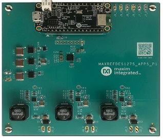
The MAXREFDES1275 has three main blocks: the microcontroller, ADC/DAC IC MAX11311, and three LED drivers. The brightness of each LED string can be set by applying an industry standard 0V to 10V dimming signal. The LED brightness should scale linearly to this signal. A conversion is required as the range and offset of the analog DIM input on the LED driver is different from this 0V to 10V signal. The microcontroller manages this by sampling the 0V to 10V DIM signals with the ADCs, calculating the new values, and forwarding them as analog voltages to the LED drivers with the DACs. A PC can be connected for a calibration procedure as the offset and maximum current can vary between the channels. The new constants are stored in the flash memory after calibration.
Features & Benefits
- Active low-fault (FLT) indicator
- Output short-circuit protection
- High-side current regulation eliminates one connection to the LED string
- 5V, 10mA LDO output provides bias to other circuits
- Ultra-low shutdown current (5μA typ)
Parts Used
Details Section
The MAXREFDES1275 has three main blocks: the microcontroller, ADC/DAC IC MAX11311, and three LED drivers. The brightness of each LED string can be set by applying an industry standard 0V to 10V dimming signal. The LED brightness should scale linearly to this signal. A conversion is required as the range and offset of the analog DIM input on the LED driver is different from this 0V to 10V signal. The microcontroller manages this by sampling the 0V to 10V DIM signals with the ADCs, calculating the new values, and forwarding them as analog voltages to the LED drivers with the DACs. A PC can be connected for a calibration procedure as the offset and maximum current can vary between the channels. The new constants are stored in the flash memory after calibration.
Its other features include:
- Active low-fault (FLT) indicator
- Output short-circuit protection
- High-side current regulation eliminates one connection to the LED string
- 5V, 10mA LDO output provides bias to other circuits
- Ultra-low shutdown current (5µA typ)
The average current-mode synchronous buck LED driver is demonstrated using the MAX20050. The LED driver runs up to 1A. Table 1 is an overview of the design specification.
| PARAMETER | SYMBOL | MIN | MAX |
| Input Voltage | VIN | 36V | 54V |
| Frequency | fSW | 400kHz | |
| Output Current | IOUT | 1A | |
This document describes the hardware in Figure 1. It provides a detailed, systematic technical guide to design an LED driver in the buck configuration using Analog Devices MAX20050 driver. The LED driver was built and tested. The details follow later in this document.
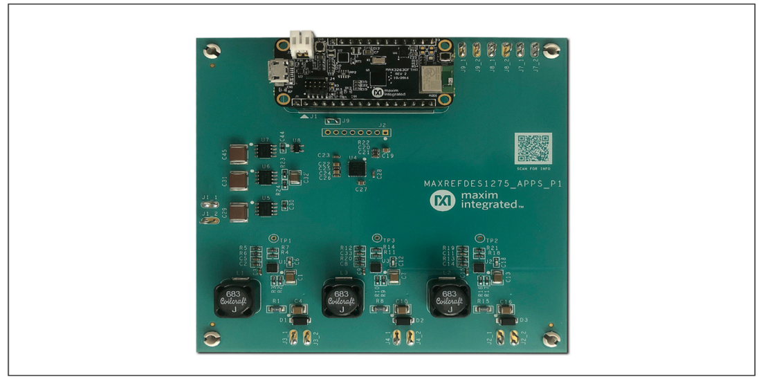
The design process can be divided into several stages: choosing the switching frequency, inductor, and capacitor, and programming the LED current. This document complements the information in the MAX20050 IC data sheet. This design uses the analog dimming control. The component design is used for all the three LED drivers for three different LED strings.
Step 1: Programming the LED Current
The MAX20050 has current sensing. It must be done on the high side of the LED current-sense resistor connected to an inductor. The other side is connected to the anode of the LED string. Refer to the application information in the MAX20050 data sheet. The LED current is programmed using RCS and the current is given by:
Equation 1:
The LED current is chosen as 1.1A. So, the RCS is 0.2Ω.
Step 2: Selecting the Inductor
The inductor is selected based on the recommendation from the Table 1 of the MAX20050 data sheet. The maximum input voltage is 54V. Hence, choose the value between 47µH to 150µH. A nominal value of 68µH is considered here.
Step 3: Selecting the Input Capacitor
The MAX20050 data sheet recommends a value of 1µF for the ceramic capacitor. The same is considered in this design.
Step 4: Selecting the Output Capacitor
Capacitance, ESR, ESL, and output ripple are the key selection parameters for the output capacitor. The MAX20050 data sheet recommends the output capacitance values based on the input voltage. A value of 0.1µF is selected here.
Step 5: Compensation
The MAX20050 has an internal loop compensation.
The MAXREFDES1275 has two main blocks: the micro-controller and LED driver sections. The microcontroller acts as a bridge between the PC and LED driver. The brightness of the external LEDs can be controlled using the serial program on the PC. The instructions are received on the serial terminal after the binary is loaded into the microcontroller. The firmware is developed using the MBED online compiler. The code can be found in the Design Resources tab.
This design has two modes: normal and calibration.
Normal Mode: The analog voltages (control voltages from the external circuit) are continuously monitored or measured by the PIXI ADC and the values are converted to DAC values controlling the LED drivers.
Calibration Mode: The system is adjusted such that the minimum (0A) and maximum LED current coincide with the minimum (0V) and maximum (10V) analog control voltage. This uses USB serial communication.
Documentation & Resources
-
MAXREFDES1275 Design Files11/21/2021ZIP951 K
Support & Training
Search our knowledge base for answers to your technical questions. Our dedicated team of Applications Engineers are also available to answer your technical questions.