
Overview
Product Details
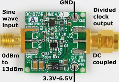
Demonstration circuit 1075B is a divide by 2/4/8 clock divider for use with high speed ADCs. Each assembly includes a clock divider followed by a re-timing stage used to produce sharp clock edges. Functionally, the DC1075B receives a high frequency sine wave which is attenuated and routed into the clock divider. The output of the clock divider is then routed to a D flip flop re-timing stage. This D flip flop is clocked by the original high frequency sine wave. This is critical to ensure signal integrity. The output of this re-timing stage is a CMOS signal suitable to be a clock source for high speed ADCs.
This circuit also is a model for designs involving FPGAs which serve as clock dividers. Whenever this is done, a D flip flop re-timing stage is required to ensure a low jitter clock signal.
Documentation & Resources
-
DC1075B Schematics5/20/2019PDF15 K
-
DC1075B Demo Manual (Rev. 0)5/20/2019PDF162 K
-
DC1075B Design Files5/20/2019ZIP1 M