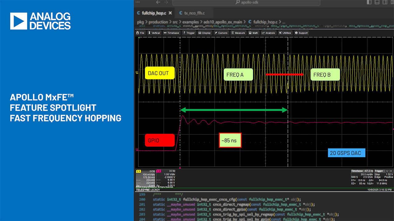
用于 16 位 2.5Gsps 高性能 DAC 的卓越时钟解决方案

设计要点 555: 引言

LTC®2000 16 位 2.5Gsps DAC 提供了较佳的 AC 性能。对于许多 DAC 应用而言,为了在不损害所关注频段之信噪比 (SNR) 的情况下实现某个频段中可用通道数目的最大化,相位噪声、噪声频谱密度 (NSD) 和无杂散动态范围 (SFDR) 指标是至关紧要的。高速 DAC 需要一个干净的采样时钟以获得较佳的噪声和杂散性能。采用具有超低噪声和杂散的 LTC6946 PLL 合成器作为用于 LTC2000 的时钟源可较大限度地提升系统性能。

Figure 1. LTC6946 Driving the LTC2000


图1:LTC6946 驱动 LTC2000


16 位高速 DAC

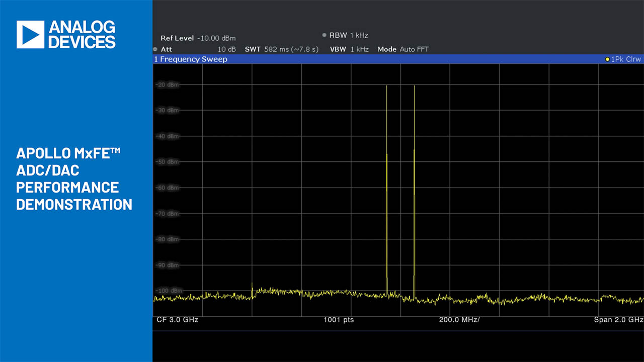
LTC2000 的高频谱纯度和低噪声特性使其成为一款超卓的信号发生器。图 2 突出显示了 LTC2000 极佳的附加相位噪声性能:当采用一个 65MHz 输出频率时,在偏移 1MHz 的情况下为 –165dBc/Hz,而在偏移 10kHz 的情况下则为 –147dBc/Hz。对于高达 100MHz 的输出频率,LTC2000 拥有优于–166dBm/Hz 的 NSD 和好于 76dB 的 SFDR。对于高达 1GHz 的更高输出频率,SFDR 超过 68dB,而且 NSD 保持低于 –155dBm/Hz。产生这些结果需要一个具有良好噪声、高频谱纯度和优异抖动性能的时钟。


作为一个时钟源的频率合成器

LTC6946 是一款具集成型 VCO 的整数 N 频率合成器,能够产生从 370MHz 至高达 6.39GHz 的信号。该器件拥有卓越的相位噪声性能和非常低的杂散分量,从而使其非常适合在 2.5GHz 频率下为 LTC2000 提供时钟。LTC6946 可直接驱动 LTC2000 (无需滤波),以产生一个频谱纯净的低噪声输出。

LTC2000 把时钟频率 (fCLK) 分频至一个输出频率 (fOUT)。该分频导致时钟的相位噪声出现在 DAC 输出端,衰减的倍数为 20 • log (fCLK / fOUT)。DAC 输出端上的总相位噪声将是 LTC2000 的附加相位噪声 (图 2) 与 LTC6946 的衰减相位噪声之组合。


Figure 2. Additive Phase Noise of the LTC2000, fOUT = 65MHz, fDAC = 2.5GHz


图 2:LTC2000 的附加相位噪声,fOUT = 65MHz,fDAC = 2.5GHz


必须最大限度地抑制采样时钟上的宽带相位噪声或抖动以避免降低 DAC 输出的 NSD,而且,LTC6946 输出的低杂散分量对于在 LTC2000 的输出端上保持高 SFDR 是至关重要的。 

相位噪声越低,由 LTC2000 生成之信号的间距就可以越紧密。这使得能够在给定的带宽内传输更多的信息。当采用一个较低的相位噪声层时,系统的总 SNR 增加,这将改善由 LTC2000 产生之信号的完整性。


结果

图 3 示出了由 LTC6946 提供时钟的 LTC2000 之单边带相位噪声。LTC6946 可与 LTC2000 很好地配合工作,产生一个干净的时钟以实现 DAC 性能的最大化。LTC2000 与 LTC6946 的组合可提供与较佳信号发生器相媲美的相位噪声和杂散性能。


Figure 3. Phase Noise of the LTC2000 Output at 80MHz Clocked by the LTC6946-3


图 3:在由 LTC6946 提供 80MHz 时钟时 LTC2000 输出的相位噪声

作者

Generic_Author_image

Clarence Mayott

Clarence Mayott is a mixed signal application section leader with over 10 years of experience at Linear Technology.

Beginning with the DC1151, a demo board for the LTC2246H, Clarence has designed nearly all of the high speed ADC demo boards for Linear Technology. These boards have been used for evaluation purposes in a wide range of applications. He designed demo boards with complete signal chains combining amplifiers and ADC combinations to help the end customer evaluate systems more easily. He also designed companion boards, including clock and signal source boards, to help facilitate the evaluation of high speed ADC demo boards. Clarence manages the continued development of PScope, the software used for various pipeline and SAR ADCs.

His expertise in design and layout of demo boards allows him to instruct customers on how to implement high speed ADCs into their own designs. He has worked on many technical areas, including medical, automotive and communications. His experience allows him to see schematic errors, minute layout errors, and other design flaws in designs.

With the release of the LTC2000, Clarence has expanded his knowledge base to include high speed DACs and waveform generation in addition to high speed ADCs. As an application section leader he oversees the continued development of LTDACGen a new software tool for generating complex waveforms for high speed DACs.

He has given technical trainings both within Linear Technology and to potential customers describing how to implement proper signal chains from the antenna through the FPGA.

He received an M.S. in Electrical Engineering from Santa Clara University and a B.S. degree in Electrical Engineering from California State University Polytechnic San Luis Obispo.