Zero-Drift Op Amps Improve Performance and Save Power
Introduction
The LTC2054 and LTC2055 are single and dual low power zero-drift operational amplifiers available in SOT-23 (LTC2054), MS8 and DD (LTC2055) packages. These are the lowest power zero-drift amplifiers available, and each offers the same high performance, including low input bias current (1pA typical), low offset (3µV max) and drift (30nV/°C max) up to 125°C while consuming only 130µA per amplifier. Similar amplifiers require 0.8mA to 1mA to achieve the same performance. Lower power consumption enables longer battery life or a greater number of amplifier functions for any system.
The SOT-23 and DD packages allow the use of either a single or dual amplifier in just 3mm × 3mm. The wide input common-mode range extends from the negative supply to 0.5V below the positive supply while the supply range runs from 2.7V to 6V for the LTC2054 and LTC2055 and 2.7V to ±5.5V for the LTC2054HV and LTC2055HV, allowing both low and high supply voltage operation.
Performance and Features
Lowest Power Across All Temperatures
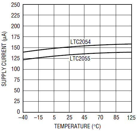
The LTC2054 and LTC2055 feature unprecedented low power dissipation, 150µA max over temp per amplifier for the LTC2055 and 175µA max over temp for the LTC2054. This is five to seven times lower power than similar amplifiers, and makes these amplifiers ideally suited for battery-powered applications such as remote sensing. System design is simplified since the supply current is nearly constant over temperature (Figure 1), unlike with other amplifiers that specify low room temperature supply current but allow much higher consumption at temperature extremes. Start-up current is also low, allowing the use of charge pumps or Zener diodes for supply regulation. Despite the low supply current, the LTC2054HV and LTC2055HV work just as well on ±5V supplies.

Figure 1. Supply current (per amplifier)
Low Input Bias Current
The LTC2054 and LTC2055 boast an incredibly low input bias current—just 1pA typical. This level of input current allows the use of large value resistors and small value capacitors without adding significantly to input offset. When used in an integrator circuit (Figure 2), the LTC2054 and LTC2055 exhibit nearly ideal DC performance. The low offset maintains output accuracy across six orders of magnitude. The low input current also minimizes input current noise and clock feedthrough.

Figure 2. Precision low drift integrator
Wide Input Common-Mode Range
In order to take greatest advantage of its low offset, typically less than 1µV, the LTC2054 and LTC2055 have high CMRR (130dB typical) over a nearly rail-to-rail input common-mode range. The common-mode range extends from the negative supply to one-half volt below the positive supply. This means that even at low supply voltages there is still a large useful input range which extends from the negative supply to above the mid-supply voltage. In addition, the common-mode range does not decrease substantially at temperature extremes as it does with most other amplifiers.
No Performance Trade-Offs
Normally, enhancements like those mentioned above require that the circuit designer give something up. Not with these devices. The LTC2054 and LTC2055 still maintain the high performance of their predecessors. High DC accuracy is retained with a best-in-class 3µV max offset spec and 30nV/°C drift. This low offset is combined with extraordinarily high CMRR and PSRR, 130dB each. High DC gain, 140dB typical, allows application in high gain circuits with low residual gain error. Noise performance is an exceptional 1.6µV peak-to-peak in 0.1 Hz to 10Hz band, and clock feedthrough is less than 0.2µVRMS, due in part to the low input currents. This level of performance is usually featured on amplifiers that require five to seven times the power of the LTC2054 and LTC2055.
All That and Small Size, Too
Many applications don’t only require precision; they need the smallest packages. In order to meet the demand for higher density, the dual LTC2055 is available in a 3mm × 3mm DD package. This allows the use of two high precision amplifiers in the same board space as a SOT-23. The LTC2054 is offered in a low-profile 5-lead SOT23 (ThinSOT™) package. Applications with limited board space need not sacrifice performance. Where space is not such a premium, the LTC2055 is also available in an MS8 package.
Applications
Current Sense Applications
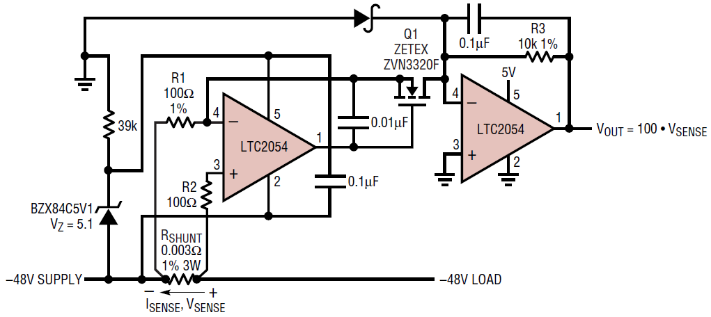
Today’s drive toward portability and power conservation has led to an interest in current monitoring. Figure 3 shows a low-side current sense circuit. In this application, an LTC2054 is used to buffer the voltage across a supply shunt resistor and convert that potential to a current using Q1. Because Q1 is in the amplifier loop, the voltage across R1 is kept equal to the voltage across the shunt resistor to within 1µV. The current is then routed through R3 via Q1 in order to level shift the output.

Figure 3. –48V low side precision current sense
A second LTC2054 sets the output reference level and R3 adds gain to the signal so that VOUT = VSENSE • R3/R1. Resistor R2 does not affect the result directly, but serves to reduce temperature-dependent voltage offsets which occur due to thermal effects on the circuit board. These offsets are usually the result of thermocouples caused by dissimilar metal junctions, such as resistor lead to solder and solder to copper trace. Additional offset may be caused by a change in resistor values or amplifier input current over temperature. Adding a matching element such as R2 helps to cancel these changes by creating symmetrical errors at the differential inputs.
DC accuracy is preserved by the extremely low input offset of the amplifiers. In addition, the low input offset of these amplifiers allows the use of a low value sense resistor, thus conserving system power. For similar systems which have supply voltages of 10V or lower, two halves of an LTC2055 or LTC2055HV may be used instead of two LTC2054s.
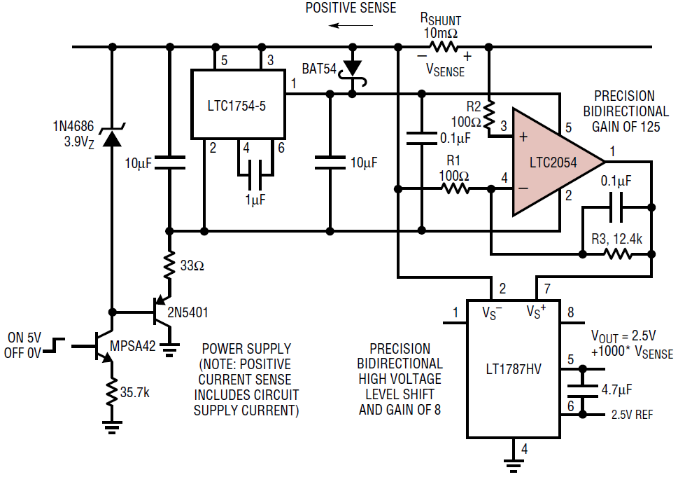
A less-obvious application for these amplifiers is a high-side current sense. Figure 4 exhibits a low power, bidirectional precision high-side current sense which can run on supplies up to 60V. This circuit uses an LTC1754-5 and a 1N4686 Zener diode to generate a high-side referred low voltage supply for the LTC2054. As with the previous circuit, the sense voltage is reflected onto R1, generating a current through R3 which is proportional to the current in the sense resistor. The LTC2054 provides, with precise gain and low offset, an output voltage that is proportional to the sense current on R3.

Figure 4. Low power, bidirectional 60V precision high side current sense
The LT1787HV level shifts the sense output to ground, and provides bidirectional output capability. The initial gain of 125 provided by the LTC2054 ensures that the accuracy is preserved despite the use of a less accurate level-shift circuit. As in the low-side current sense circuit, the low input offset of the LTC2054 allows the use of a small sense resistor without giving up precision, even with relatively low shunt currents.
Photodiode Amplifier
Figure 5 illustrates a circuit that uses an LTC2054 as a transimpedance amplifier. The current in a photodiode is converted to a voltage at the output. The low input bias current and input noise current, combined with low voltage offset, provide a precision signal monitor. A high degree of input sensitivity is provided to the circuit by the large dynamic range, characterized by low input offset and high DC gain of the LTC2054. In addition, the LTC2054HV allows ±5V supply operation, further increasing dynamic range.

Figure 5. Ultra-precision, wide dynamic range 10Hz bandwidth photodiode amplifier
Conclusion
The LTC2054 and LTC2055 low drift operational amplifiers couple low power consumption with high precision DC specifications. They require little board area, available in small footprint packages including SOT-23-5 for the LTC2054 and the industry-leading 3mm × 3mm DD package for the LTC2055. A wide input common-mode range and a wide supply range that allows operation between 2.7V and ±5V provide flexibility.


