摘要
This technical note is focused on how to determine the system specification of a CDMA receiver in order to establish a practical specification for a low noise amplifier and down converter. In the second section, the performance and features of MAX2323/25/29 are described in detail. The last section provides details of how to design the receiver front end, including designing matching circuits for RF and IF SAW filters to optimize performance of the receiver. A practical circuit and measurement data are shown in this note as well.
Additional Information:
Introduction
RF designers developing a second- or third-generation CDMA cellular phone or wireless modem often meet a challenge in choosing a front-end chip set with the best performance to meet their system specification. Maxim Integrated provides some of the best choices: MAX2323/2325/2329. These are LNA/Mixer ICs optimized for CDMA applications in both cellular and PCS bands. The MAX2323 addresses dual-band, triple-mode CDMA applications by providing switched signal paths for cellular CDMA and PCS CDMA. The MAX2325 and MAX2329 are cellular-band dual-mode and PCS-band versions, respectively.
This technical note is focused on how to determine the system specification of a CDMA receiver in order to establish a practical specification for a low noise amplifier and down converter. In the second section, the performance and features of MAX2323/25/29 are described in detail. The last section provides details of how to design the receiver front end, including designing matching circuits for RF and IF SAW filters to optimize performance of the receiver. A practical circuit and measurement data are shown in this note as well.
RF CDMA Receiver System Requirements and Issues
Wireless code division multiple access (CDMA) networks, based upon the IS-95 standard and protocol developed by Qualcomm, are being deployed worldwide. Today's second and third generation CDMA phone standards vary widely based upon the country or region. The first standardization phase for upcoming third-generation (3G) wireless communications is coming to an end. It is certain CDMA cellular phones will be one of major cellular phones in next a few years on the market.
The harsh wireless environment, in which these CDMA mobile stations or phones must coexist with other multi-standard mobile phones, impose tough system conditions on the radio. These conditions demand a high performance RF front end and DSP back end.
CDMA Receiver Sensitivity and Dynamic Range
Before starting to specify the noise figure and third intermodulation characteristics of a LNA and a mixer, we should understand narrow band CDMA and wide band CDMA receiver system specifications. In the IS-98A/95B and interim standard, the RF receiver sensitivity of the CDMA cellular mobile station is defined at the mobile station antenna connector. It is equal to the minimum received forward CDMA channel power,  , at which the frame error of the receiver does not exceed 0.5%. The minimum required sensitivity for the received forward channel as equal to -104dBm. The maximum input power is -25dBm.
In the case of the receiver, there are two sources of interference that are purely white Gaussian noise:
- The receiver's input referred thermal noise power spectral density No.
- The transmitter's thermal noise power spectral density in the receive frequency band, Ntx (see reference 1,2).
No is determined by the receiver's noise figure (NF), and Ntx is determined by the amount of transmitter's output thermal noise leaking to the mobile station receiver's input through the duplexer. A typical Power amplifier has an output thermal noise power spectral density in the receiver frequency band of -135dB/Hz. Assuming a minimum of 43dB attenuation through the duplexer from transmitter to antenna input in the receiver band, Ntx can be calculated as -178dBm/Hz at the mobile station antenna connector. If this effect is considered, 2dB of margin is needed to add to the effective ratio Eb/Nt as
 = 6.5dB
It should be noted that the IS-98A standard specifies that the minimum traffic channel  should be equal or greater than 4.5dB if frame error rate (FER) meets 0.5% when assuming an information rate of 9600. That requires the minimum sensitivity of traffic channel to be changed from -104dBm to P (actual) = -106dBm. Then minimum receiver noise figure NF can be deduced as:
NF = P (actual) - 10log (K×To×BW) = -106dBm + 113dBm = 7.8dB (2)
Where, K is Boltzman's constant, To is standard noise temperature and BW is1.23MHz channel bandwidth for narrow band CDMA. This NF requirement is for the entire receiver. Subtracting the loss of 0.5dB in the diplex circuit and 3.5dB in the duplex circuit, the NF requirement for the rest of the receiver is 3.8dB. From the system simulation of the receiver, NF of a LNA for cellular band should be less 2dB, and 2.3dB in PCS band.
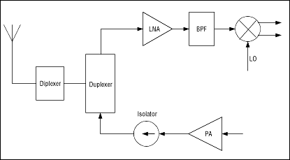
The front-end gain must be high enough to overcome the noise contribution of the following circuits, which may otherwise degrade the receiver's sensitivity. This gain is constrained by the strong out of band unwanted signals and the linearity of the following circuits. If the front-end gain is too high, the mixer will overload and compromise the performance. An LNA with a 14dB to 16dB gain step is a proper selection for both bands.
Information data in a CDMA system is bi-phase modulated. The resultant modulated signal envelope is not constant, and the typical peak to average ratio for a narrow band CDMA could be close to 10dB. Peak to average ratio for WCDMA could be close to 12dB. As result, for proper received signal detection and demodulation, the mobile station receiver should stay linear under the allowable received signal input power range. Normally, 90dB of dynamic range is required for the receiver. From a linearity point of view, the mixer input 1dB compression point is the main system limiter in a CDMA receiver design for high level (-30dBm to -20dBm) received signals. In order to resolve this problem and design a practical mixer, the front end LNA needs to extend the dynamic range by 15dB. This is accomplished by a low gain mode with a gain reduction between 15dB to 20dB.
Input Third-Order Intercept Point (IIP3) of the LNA and the Mixer
The adjacent channel selectivity is a measure of the ability of the receiver to detect the desired modulated signal without exceeding a given degradation due to the presence of an unwanted signal in the adjacent channel. The receiver must maintain a frame error given by the standards.
The intermodulation response attenuation is a measure of a receiver's ability to receive a cellular band CDMA signal on its assigned channel frequency in the presence of two interfering continuous wave (CW) tones. Theses tones are separated from the assigned channel frequency and from each other such that the third order intermodulation product of two tones produces an in-band interfering signal to the desired signal due to non-linearity of LNA and mixer. IS-98A standard calls for three different cases of different two-tone levels and desired signal levels, under which the FER should not exceed 1% and  should be 4.3dB. It is supposed that 1.5dB margin is added for traffic channel system consideration, and then
  is required as above 5.8dB. In the small two tone level case, the equivalent white noise interference source Ioc consists of the receiver's thermal noise No and the transmitter's thermal noise in the receiver band Nt, and an equivalent in-band interference component due to the third order intermodulation product IIM3. In a 1.233MHz bandwidth, Ioc should not exceed -101.3dB. IIM3 can be expressed in linear form as:
IIM3 = IOC -(No + Nt) × BWRF (3)
Where No is set by -166.2dBm/Hz and Nt is set by -178dBm/Hz. From equation (5), IIM3 should be less than -103.7dBm/1.23MHz. As a result, IP3 in the small two-tone level's case should be greater than -12.7dBm by using formula (4).
IIP3 = Pin + ΔIM3 / 2 (4)
Where Pin is set by -43dBm (IS-98A) for two tones and ΔIM3 is set by 60.7dBm (-103.7dBm+43dBm). In the large two tone case, the desired CDMA signal level is 25dB above the minimum receiver sensitivity level. The equivalent in-band white noise interference source is totally dominated by the third order intermodulation product IIM3 when the power level of two tones is -21dBm as IS-98A standard requires. This means that IIM3 is equal to Ioc and should not exceed -79.3dBm/1.23MHz. Similarly, 1.5dB margin is added for  =5.8 dB. The third order intermodulation spurious response attenuation ΔIM3≥ 58.3dB. This case requires the IIP3 of the LNA should exceed +8.5dBm for large two tones case. Following the IS-98A standard requirement, there are three two-tone test cases, the middle power level of two tones is -30dBm. This means that the LNA of the cellular band needs variable gain control or three linearity modes to handle the third order intermodulation issues.
Single-Tone Desensitization
The desensitization characteristic of the receiver determines its ability to operate successfully under strong interferers. They are specified separately for in-band and out-of-band conditions. In the cellular band and PCS band, the single tone desensitization is a measure of the receiver's ability to receive a CDMA signal, at its assigned channel, in presence of a single tone with -30dBm power and spaced at a given }900KHz frequency offset from the cellular band desired signal frequency center and }1250KHz frequency offset from the PCS band desired signal frequency center. As defined in the IS-98A and IS-98B standard, the receiver error rate should not exceed 1% ,  = -101dBm/1.23MHz, and
  should be 4.3dB. As was done before, it is assumed that a 1.5dB margin is added for traffic channel system considerations, and then
  is required as above 5.8dB. The equivalent white noise interference at the mobile station antenna is defined as
Ioc = Is + (No + Nt) × BWRF (5)
Where Is is equivalent in-band interference component due to single tone jamming. If the noise figure of the receiver (NF) is chosen as 7.8dB, No is set to -166.2dBm/1.23MHz and Nt is equal to -178dBm/1.23MHz. From equation (7), Is should be less than -103.7dBm/1.23MHz. The single tone generates two interfering components. The first one caused by the single tone jamming results from the reciprocal mixing phenomena, denoted by IMIX. It occurs when the forward received signal suffers from the interference due to receiver RF VCO phase noiseΦN mixing with the single jamming tone and mixing down to the IF. The second interference component caused by the single jamming tone results from the cross modulation phenomena, denoted by IMOD. It occurs when the envelope modulation of transmited power leaks from the power amplifier to the LNA input through the duplexer's isolation. Cross-modulation in the LNA will generate an in-band interference to the received forward CDMA channel signal, at the LNA output ³. Reference article #3 provides a typical value ofMIX = -105.6dBm/1.23MHz and based on typical phase noise of -137dBc/Hz at 900KHz offset for cellular band and integrated phase noise ΔΦN = -75.6dBc. Is should be lower than -108.2dBm/1.23MHz. For a cellular CDMA receiver, one can assume that all cross modulation happens in the LNA. This requires the IIP3 of the LNA meets:
IIP3LNA = 1/2 (2 × PTX + PST_LNA - IMOD_LNA - 3) (6)
Where PTX is transmit leakage power level at LNA input, PST_LNA is jamming tone power level at LNA input and IMOD_LNA is cross-modulation power. It is assumed that the power amplifier output power is +28dBm and the RX to TX duplexer isolation is -58dB, resulting PTX = -30dBm. The power of single tone PST_LNA is -33dBm due to 3dB loss of the duplexer. IMOD_LNA should not exceed -111.2dBm/1.23MHz in order for the receiver to meet the required performance at the correlator output  ≥ 5.8dB. From equation (6), the third order intermodulation point of LNA input should be greater than +7.6dBm based the above assumption.
Second-Order Intercept Point of the LNA and the Mixer
Low even-order distortion, especially second order distortion, is crucial to the receiver's performance in the presence of strong signals with time-varying envelopes. When a second-order nonlinearity is exposed to such a signal, a spurious base band signal proportional to the squared envelope is generated at base band, which disturbs the reception of the desired signal. Two such groups of disturbing signals are present: unwanted channels in the receive band (forward channel) and the transmitter leakage signal. The spectral shape of these disturbing signals is the same as the desired signal, but the spectral content of the second order product has a DC component and a much broader frequency span than the desired baseband signal. Typically, the DC component represents half the power while other half of the power lies above the desired signal bandwidth. In the CDMA system, especially in the PCS band, where RF bandwidth of the receiver is 60MHz, a single jamming tone with a frequency lying at fRF 1/2± fIF will be down converted to the IF due to the second order product of the mixer. In this case, the equivalent white noise interference source Ioc consists of No, Nt and the equivalent in band interference component due to the _ IF spurious mixer product (Ist). If 1dB margin is added, then  equals to 5.3dB. We can deduce that Ist ≤ -102.9dBm/1.23MHz. Here Ist is the equivalent interference level referred to the receiver's input due to a single jamming tone.
Allowing 6dB loss from the antenna connector to the input of the mixer and 14.7db of PCS LNA gain results in the single jamming tone (Pj) having -24dBm power input to the mixer and Ist has -94.2dBm/1.23MHz power input to the mixer. Therefore, Δ1/2IF = 70dBc spurious product suppression is required. The requirement of suppressing 1/2 IF spurious for second order interception IIP2MIXER is ³.
IIP2MIXER ≥ Pj + Δ1/2IF = -24dBm + 70dBm = + 46dBm (7)
Since the transmitter signal is always present, the second order products should be sufficiently suppressed (for example, 10dB below the noise level). As in the above discussion, PTX = -30dBm , cascaded gain from Antenna connector to the mixer input is 8.7dB for the desired signal and -5 loss for TX leakage signal. Given an acceptable input level P (actual) = -106dBm, a rough estimate of IIP2MIXER can be determined.
IIP2MIXER ≥ 2 (PTX -5) - [P (actual) + 8.7 -10] = 2 (-30-5) dBm - (-106 + 8.7 - 10) dBm = + 35.3dBm (8)
Low-Noise Amplifier and Downconverter with High Performance and Low Cost
The low noise amplifier and mixer represent one of the basic building blocks of a receiver in a mobile station. In real-world situations, the desired received signal could be very low in power and must be amplified. Today's digital communication systems with high data rates and large bandwidth requirements demand LNA and down-converter designs with increasing dynamic range. The challenge to RFIC designers and semiconductor device technologists is that these conditions must be met with constantly decreasing size, power levels and manufacturing costs. The primary design goals for a LNA are:
- Achieve high gain and low noise.
- Achieve high IIP3 and low power consumption.
Figure 1 is a block diagram of MAX2323 chip. To optimize cellular band dynamic range at minimum current, the MAX2323/25 implements four LNA states: high-gain/high-linearity; high-gain/low-linearity; mid-gain, and low-gain. In the high-gain/high-linearity mode, the adjustable high intercept LNA minimizes desensitization in the presence of a large interfering signal. For the other gain states, the LNA current is reduced to improve standby time.
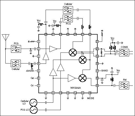
Figure 1. Block diagram of the MAX2323.
The CDMA mixers are designed for high linearity, low noise, and differential IF outputs, while the FM mixer is designed for lower current and single-ended output. Each band is implemented with a separate mixer to optimize performance for the specific band.
Performance improvements in silicon ICs have been largely achieved via reduction in geometry and corresponding low energy implantation processes. Maxim employs SiGe (graded-base) technology, where incorporation of germanium into the base region of the transistor opens up new avenues to the device designer to improve frequency response, gain and linearity without the standard constraints of an implanted process. The cutoff frequency fT, a key figure of merit of a transistor in MAX2323 is up to 35 GHz. The designers of MAX2323/2325/2329 have taken a lot new approaches to optimize the performance of ICs. The reader can look at tables below that give details of DC and AC electrical characteristics of MAX2323/2325/2329.
DC Electrical Characteristics
(VCC = 2.7 to 3.6V, RBIAS = 20kΩ, RLNA = 24kΩ, TA = -40 to + 85°C, typicals are at 2.75V and 25°C, unless otherwise noted.) All DC parameters are 100% production-tested at room and hot temperatures.
| PARAMETER | CONDITIONS | MIN | TYP | MAX | UNITS |
| PCS CDMA Mode (MAX2323) |
|||||
| Operating supply current | Midgain mode | 20 | 22 | mA | |
| Operating supply current | High-gain low-linearity idle mode |
21 | 24 | mA | |
| Operating supply current | High-gain high-linearity mode | 25 | 28 | mA | |
| Cellular CDMA Mode (MAX2323 and MAX2325) | |||||
| Operating supply current | Low-gain mode | 17.5 | 20 | mA | |
| Operating supply current | Midgain mode | 19 | 21.5 | mA | |
| Operating supply current | High-gain low-linearity idle mode |
19 | 21.5 | mA | |
| Operating supply current | High-gain high-linearity mode | 26 | 29 | mA | |
| FM Mode (MAX2323 and MAX2325) | |||||
| Operating supply current | Low-gain mode | 14.5 | 17.5 | mA | |
| Operating supply current | Midgain mode | 16 | 19 | mA | |
| Operating supply current | High-gain low-linearity mode | 16 | 19 | mA | |
| Shutdown Mode | |||||
| Shutdown supply current | SLEEP = High | 1.8 | 35 | µA | |
| All Modes | |||||
| Digital input logic high | Except SLEEP input | 2.0 | V | ||
| SLEEP input logic high | VCC -0.6 |
V | |||
| Digital input logic low | 0.6 | V | |||
| Digital input current | 6.5 | µA | |||
| Digital input current | -35 | µA | |||
AC Electrical Characteristics
(MAX2323/2325 EV-kit, FPLNAIN = 1960MHz, FCLNAIN = 881MHz, FIF = 110MHz, High-side LO, 50Ω system, RBIAS = 20kΩ, RLNA = 24kΩ, VCC = 2.75V, TA = 25°C, LO input power = -7dBm, LOW = 0V, HIGH = VCC, unless otherwise noted.) AC performance is measured on three lots with min/max limits set at +/- 3. Gain is production-tested at room and hot temperatures for functionality only.
| PARAMETER | CONDITIONS | MIN | TYP | MAX | UNITS |
| OVERALL PERFORMANCE | |||||
| Low-band RF frequency range | Note 1 | 850 | 950 | MHz | |
| High-band RF frequency range | (MAX2323), Note 1 | 1800 | 2200 | MHz | |
| Low-band LO frequency range | Note 1 | 800 | 1150 | MHz | |
| High-band LO frequency range | (MAX2323), Note 1 | 1600 | 2300 | MHz | |
| IF frequency range | Note 1 | 40 | 400 | MHz | |
| LO input level | 100Ω input impedance | -7 | -5 | 0 | dBm |
| LO emissions at CLNAIN | Interstage filter rejection = 20dB, LOLIN = -5dBm |
-55 | dBm | ||
| LO emissions at PLNAIN | Interstage filter rejection = 20dB, LOHIN = -5dBm |
-55 | dBm | ||
| LNA PERFORMANCE | |||||
| Cellular LNA Performance (MAX2323 and MAX2325) | |||||
| CDMA High-Gain High-Linearity Mode | |||||
| Gain | TA = TMIN to TMAX | 14.5 | 15.5 | 17 | dB |
| Noise figure | 1.7 | 1.9 | dB | ||
| IIP3 | 9 | 10.5 | dBm | ||
| CDMA High-Gain Low-Linearity Paging Mode, and FM High-Gain Mode | |||||
| Gain | TA = TMIN to TMAX | 13 | 14.5 | 16 | dB |
| LNA noise figure | 1.7 | 1.9 | dB | ||
| LNA IIP3 | Note 4 | 3.5 | 5 | dBm | |
| CDMA and FM Midgain Modes | |||||
| Gain | TA = TMIN to TMAX | 4.5 | 6 | 8 | dB |
| Noise figure | 3.3 | 3.5 | dB | ||
| IIP3 | Note 4 | 8.5 | 10 | dBm | |
| CDMA and FM Low-Gain Modes | |||||
| Gain | TA = TMIN to TMAX | -4.5 | -3.5 | -1.5 | dB |
| Noise figure | 7.3 | 8 | dB | ||
| IIP3 | Note 4 | 13 | 17.5 | dBm | |
| PCS LNA Performance (MAX2323) | |||||
| CDMA High-Gain High-Linearity Mode | |||||
| Gain | TA = TMIN to TMAX | 13.5 | 14.5 | 15.5 | dB |
| Noise figure | 2.0 | 2.2 | dB | ||
| IIP3 | 7 | 8 | dBm | ||
| CDMA High-Gain Low-Linearity Paging Mode | |||||
| Gain | TA = TMIN to TMAX | 12.5 | 13.9 | 14.5 | dB |
| LNA noise figure | Note 2 | 2.0 | 2.1 | ||
| LNA IIP3 | Note 4 | 4.5 | 5.5 | dBm | |
| CDMA Midgain Mode | |||||
| Gain | TA = TMIN to TMAX | -2.0 | -1.0 | -5 | dB |
| Noise figure | Note 2 | 5.6 | 6.0 | dB | |
| IIP3 | Note 4 | 12 | 13.5 | dBm | |
| MIXER PERFORMANCE | |||||
| Cellular Mixer Performance (MAX2323 and MAX2325) | |||||
| CDMA, All Modes | |||||
| Gain | TA = TMIN to TMAX | 11.5 | 12.8 | 14.5 | dB |
| Noise figure | 7.5 | 8.5 | dB | ||
| IIP3 | Note 4 | 3.5 | 4.8 | dBm | |
| FM Mode | |||||
| Mixer gain | TA = TMIN to TMAX | 8.5 | 10 | 11.5 | dB |
| Mixer noise figure | 10.5 | 11.5 | dB | ||
| Mixer IIP3 | Note 4 | 2.5 | 5 | dBm | |
| PCS Mixer Performance (MAX2323) | |||||
| CDMA High-Gain High-Linearity Mode | |||||
| Gain | TA = TMIN to TMAX | 12 | 13.5 | 15.5 | dB |
| Noise figure | 7.9 | 8.5 | dB | ||
| IIP3 | Note 4 | 2.5 | 3.9 | dBm | |
| Half-IF spurious response | Note 5, 2x2 intercept point | 47 | dBm | ||
Notes
Note 1. Operation over this frequency range requires the ports to be rematched for the desired operating range. Performance at various frequencies is indicated by the S-parameter data.
Note 2. Noise figure is measured with an inductor of Q = 40 in the input impedance matching circuit.
Note 3. Specs are based on RBIAS = 20kΩ. Icc for all LNAs (except HGHL) and mixers are inversely proportional to RBIAS. IIP3 can be traded for Icc by selecting other values for RBIAS. The relation is approximately a 3dB change in the IIP3 for a factor of 1.4 change in current.
Note 4. FLO = 2040MHz, FRF = 1985MHz at -35dBm, POUT measured at 110MHz. Specification is calculated as: _IF IIP = 2*PRF - (POUT - Gain) (in dB).
From the above tables, note that the LNA has three gain modes to handle different RF input power levels and jamming signals. Typically the cellular band LNA has 1.7dB noise figure and 15.5dB gain and +17.5dBm IIP3 in low gain mode. In the PCS band the LNA has 2.0dB noise figure and 14.5dB gain and +13.5dBm IIP3 in middle gain mode.The mixers in both bands with 12.5 to 13.5dB gain meet the minimum system specifications. The test data shows that 1/2IF IIP of the mixer is better than +47dBm in PCS band that meets basic system requirement of suppressing 1/2IF interference.
Front-End Receiver with the MAX2323
It is a big challenge for a RF design engineer to design optimal circuits with low cost and layout a PC board in limited space for a dual-band triple mode cellular phone based on given available front-end chip sets on the market. The basic steps for designing a RF receiver can be summarized as follows.
RF System and Architectural Design with the System's Performance Analysis and Simulation
When developing a front-end schematic for a receiver one of most important things is to understand how to define the RF system specification based on given system standards and product requirements. An architecture of the transceiver with an optimal frequency plan and block diagram needs to be carefully generated in order to set the specification for each block, IC and modules. The goal is to reduce the cost, increase receiver sensitivity and reduce the call-drop rate. At this stage, it is necessary to establish a link budget with a spreadsheet for determining the noise figure, gain, IIP2 and IIP3. A good approach is to employ a powerful RF/Microwave CAD tool such as HP ADS to do simulation and analysis for optimizing each block's performance. Based on the system performance simulation, it is found that MAX2323 is one of the best available chips on the current market, which meets all the system specifications in both bands. It has been widely employed by many cellular phone designers now because of its low cost, high performance and high stability. It should be pointed out that there are a lot of trade-offs in RF system design based on the differing requirements of low tier and high tier cellular phone products.
Selection of IF Frequency for the Cellular Band and the PCS Band
Selecting an optimal intermediate frequency for the receiver is an important issue for a RF receiver designer. In general consideration, a half IF issue should be avoided if the down-converter is not capable of suppressing the spurious response much lower than the desired IF signal level. Normally the intermediate frequency of a the PCS band should be above 120MHz, and it should be above 50MHz in the cellular band due to the 1/2 IF offset issue. 85.38MHz IF SAW filter is commonly used in a cellular band receiver and 210.38MHz IF SAW filter is selected for the PCS band. These IF approaches are not unique approaches for cellular phone receivers. Since a high performance IF SAW filter can not be replaced by any other available filters in CDMA mobile stations today, we can not save such components but we can reduce the amount of SAW filters if a proper down-converter with LNA and proper IF are properly selected.
Theoretically, the transmitter does not need a relatively high cost IF SAW filter to suppress spurious signals and the noise floor. It is therefore possible to use two different IFs in transmission and one IF frequency can be employed in reception when a dual band receiver is designed and cost is a top priority. The MAX2323 has no problem with the half IF issue, so any available IF SAW filter such as 85.38MHz or 180MHz SAW filter (applied for current mobile stations), can be employed without any technical limitations. If a designer does prefer to use two IFs for different bands (expect a 1% to 2% increase with the addition of 1 more IF SAW filter.), a band switch is recommended on the differential output of MAX2323 mixer. A typical application schematic of MAX2323 is shown on Figure 2. It should be pointed out that the input and output impedance of all ports in Figure 2 are tuned to 50Ω for the testing purposes, where the IF is 85.38MHz.
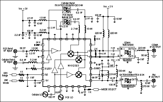
Figure 2. Application circuit of the MAX2323.
Optimizing the Matching Network for the LNA and the Downconverter
The matching circuits of the RF image SAW filter and the IF SAW filter play a crucial role in cellular phone designs. In particular, IF SAW filters in cellular and PCS receivers are required to reject out of band interference with minimal amplitude and phase distortion of the in-band signal. When the matching networks for the LNA and down converter are designed, the complete S-parameters of the LNA, mixer, RF image filter and IF SAW filter are required. There are many textbooks and articles that have discussed how to design the matching network. The fundamental issue is how to trade off among the maximal LNA gain and mixer's gain, the noise figure of LNA and the IIP3 of the mixer. Since parasitics and mutual inductance exist between inductors, and the SAW packages are sensitive to layout details, performance cannot be accurately predicted or modeled. Furthermore, accurate measurements of the SAW impedance are difficult to achieve. Therefore, an accurate impedance model is essential in determining a matching topology that has minimal negative impact on performance. This requires a practical model for each particular design project and matching network.
The main design goals of a LNA are to achieve high gain and low noise. Optimization of the impedance match for gain of the LNA almost always guarantees non-optimal values for the noise factor. The designer must replace ideal sources in bias circuits and ideal values in the matching circuit with equivalent real components, valid over the frequency range of interest. The MAX2323 requires two resistors (connected to pin 1 and pin 2) for bias setting which may also alter the linearity of the input LNA. For nominal bias, a 24KΩ resistor is connected to pin 1 and 20KΩ resistor is connected to pin 21. The matching networks for the LNA consist of inductors and capacitors. The finite Q of inductors and capacitors must be considered when using inexpensive (lossy) components in the design. After establishing the matching network, the designer still needs to make some modifications on the matching network when trading off gain and return loss. The typical return loss for the LNA requires that S11 and S22 should be less than -10dB.
The MAX2323 has two IF outputs. One is the differential output port for the CDMA mode. Two pull-up inductors and two blocking capacitors are required which are used as part of the IF matching network. The output impedance of this port is 2.4KΩ. The other output is the single ended IF output port. It requires a pull-up inductor and a DC blocking capacitor which are used as part of the matching network. In general, the input impedance of the IF SAW Filter in each of two modes is not matched with MAX2323 IF output port. An impedance transfer network should be inserted between the down-converter and the IF SAW filter. In Figure 2, there is a Thomson IF CDMA SAW filter with 400Ω equivalent input/output impedance and a MuRata FM IF SAW filter with 1KΩ input/output impedance. A simulation for the IF matching network can be done by HP-ADS tools, where the S-parameters of selected the SAW filter needs to be inserted in the circuit. It is necessary to note that obtaining high conversion gain from the down-converter to IF SAW filter output does not result obtaining a high IIP3 of the mixer. Carefully tuning the value of each capacitor, resistor and inductor in matching network is absolutely required in order to obtain an optimal IIP3 and conversion gain of the down-converter in the MAX2323.
The following tables give the test data obtained from a real PCB of a cellular phone. The measurement indicates that cascaded NF from LNA input to output of IF SAW filter is 2.51dB in high gain CDMA mode and 15.3dB cascade gain with the 10dB insertion loss of the IF SAW filter.
| MODE | HGHL | HGLL | MIDDLE GAIN | LOW GAIN | |
| Current @ +3.0V | 25.5 | 18.7 | 18.7 | 17.1 | mA |
| Gain @ 880MHz | 14.8 | 13.6 | 5.2 | -4.0 | dB |
| NF @ 870MHz | 1.77 | 1.83 | 3.50 | 7.50 | dB |
| NF @ 870MHz | 1.80 | 1.90 | 3.60 | 7.44 | dB |
| NF @ 870MHz | 1.85 | 1.95 | 3.58 | 7.60 | dB |
| IIP3 | 11.0 | 5.5 | 10.5 | 19.2 | dBm |
| NF (dB) | 2.5 | Gain | +1.7dB |
| Gain (dB) | 15.3 | NF | 9.0dB |
| IIP3 (dBm) | -10.5 | IIP3 | +4.1dBm |
| IMAGE FILTER | TMX M300 | |
| NF (dB) | 2.5 | 10 |
| Gain (dB) | -2.5 | -10 |
| IIP3 (dBm) | 100 | 100 |


