Triple and Quad RGB Amplifiers Deliver Full Performance on 3.3V
Introduction
The LT6550 and LT6551 3.3V triple and quad high speed amplifiers make it possible to create compact solutions for driving RGB and component video cables. These voltage feedback amplifiers drive either 50Ω or 75Ω double terminated cables and are preconfigured for a fixed gain of two, thus eliminating six or eight external gain setting resistors.
The industry trend of using lower supply voltages increases the demands placed on analog signal handling characteristics. For example, a 3.3V video amplifier not only requires high slew rates and fast settling times but must also have wide input and output voltage swing ranges to avoid clipping any portion of the video waveform. Current feedback amplifiers cannot be used because they lack sufficient signal swing at low supplies and they require input signal above ground.
The LT6550 and LT6551 are true voltage feedback amplifiers featuring 110MHz (–3dB) bandwidth, 340V/μs slew rate, and fast settling time, making them ideal for low voltage, high resolution, RGB Video Processing.
The LT6550 and LT6551 operate from 3V to 12.6V and are fully specified on single 3.3V and 5V supplies, the LT6550 is also fully specified on ±5V supplies. Both parts are available in compact 10-pin MSOP packages and performance is guaranteed over the industrial temperature range.
Amplifier Characteristics
The block diagrams in Figure 1 show the differences between the LT6550 and LT6551. The LT6551 quad is designed for single supply operation with the feedback returned to ground. The LT6550 triple has a separate VEE pin and can be used on either single or split supplies.
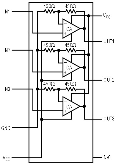
Figure 1a. LT6550 block diagram.
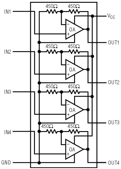
Figure 1b. LT6551 block diagram.
These devices feature internal feedback resistors and a flow-thru pin out, which simplifies PC board layout and enhances performance by minimizing input to output stray capacitance. The amplifiers feature a rail-to-rail output and an input common mode range which includes ground. Figure 2 shows the output swing driving a 150Ω load vs supply voltage. On a single 3.3V supply, the input voltage range extends from ground to 1.55V and the output typically swings to within 400mV of the supply voltage while driving a 150Ω load. Table 1 summarizes the major performance specifications.
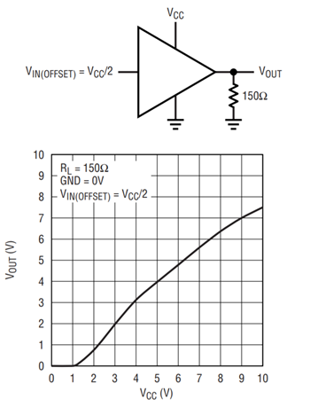
Figure 2. Output swing high vs supply voltage.
| Parameter | Conditions | Typical Values@3.3V/0V | Typical Values@ 5V/0V |
| –3dB Bandwidth | RL = 150Ω | 90MHz | 110MHz |
| 0.25dB Gain Flatness | RL = 150Ω | 30MHz | 30MHz |
| Output Voltage Swing High | RL = 150Ω | 2.5V Minimum | 3.5V Minimum |
| Output Voltage Swing Low | ISINK = 10mA | 200mV Maximum | 200mV Maximum |
| Slew Rate | RL = 150Ω | 250V/μs | 340V/μs |
| Settling Time to 3% | VOUT = 1.5V step, RL = 150Ω | 20ns | 20ns |
| Channel Separation | Between all Channels at 10MHz | –60dB | –60dB |
| Differential Gain | RL = 150 | 0.09% | 0.05% |
| Differential Phase | RL = 150 | 0.09° | 0.05° |
| Supply Current per Channel | 8.5mA | 9.5mA |
Figure 3 shows a simplified schematic of one channel of the LT6551. Resistors RF and RG provide an internal gain of 2. (The LT6550 triple is a slight variation with the gain setting resistor, RG, connected to a separate ground pin). The input stage consists of transistors Q1 to Q8 and resistor R1. This topology allows for high slew rates at low supply voltages. Transistors Q3 and Q4 are class AB biased as are transistors Q5 and Q6. The input stage transconductance is derived from 1/gm of these transistors and resistor R1. The input stage drives the folded cascode degeneration resistors of PNP and NPN current mirrors, Q9 to Q12, which convert the differential signals into a single-ended output. There are back-to-back series diodes, D1 to D4, across the plus and minus inputs of each amplifier to limit the differential input voltage to ±1.4V. RIN limits the current through these diodes if the input differential voltage exceeds ±1.4V. The complementary drive generator supplies current to the output transistors that swing from rail-to-rail.
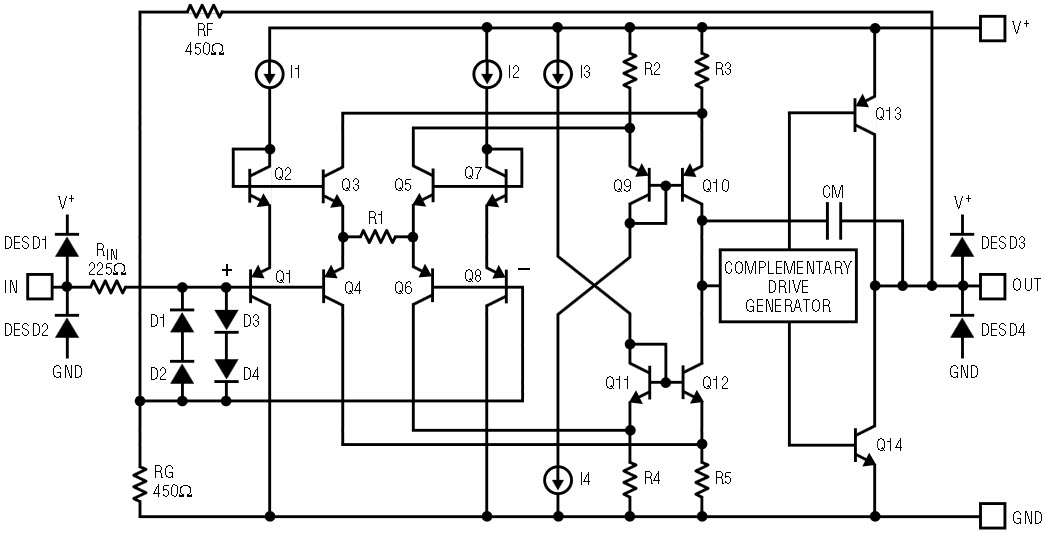
Figure 3. Simplified schematic.
RGB Video Applications
RGB (Red, Green, and Blue) video format requires three signals that represent the amplitudes of the respective colors plus timing signals (sync) that are sometimes combined with the green component.
With video amplifiers driving double terminated 50Ω or 75Ω cables, the video output taken from the far end of the cable is 6dB lower than the output of the amplifier. For this reason these video amplifiers are configured for a closed loop gain of +2. The black (lowest output for all three colors) to white (highest) voltage range for each of the respective RGB channels is approximately 700mV, sync pulses are typically 300mV lower than the black level resulting in a total voltage range of 1.0V. This means that for DC-coupled applications, the output of the amplifier needs to swing at least 2.0V while driving a 150Ω load and the input range should be greater than 1.0V. The LT6550 and LT6551 were designed to meet these requirements.
Figure 4 shows a 3.3V powered RGB cable-driver application that could handle additional sync information on any channel. Using DC-coupled inputs allows precise control of the signal swing within the guaranteed 2.3V available output range. For applications that require a separate sync output, the fourth channel of the LT6551 can be utilized as shown in Figure 4.
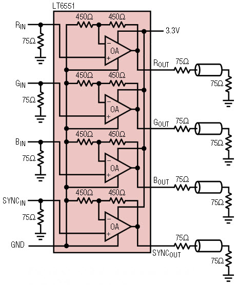
Figure 4a. 3.3.V single supply RGB plus SYNC cable driver.
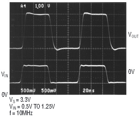
Figure 4b. Output step response.
AC Coupled S-Video Splitter
The S-video format separates the luma signal (Y) from the chroma subcarrier signal (C), and is usually AC-coupled. AC-coupled applications require the design to accommodate picture-content offset in the signal by allowing output swing of 3.2V for composite or 2.5V for sync-stripped video.
Figure 5 shows an AC-coupled luma and chroma channel video cable driver that provides dual Y and C output ports. Operating from a single 5V supply, the LT6551 provides a guaranteed output swing of 3.3V, with the bias point established by the input resistor network shown. The chroma signal is a color subcarrier signal with no picture content offset, so it is readily accommodated with the same biasing scheme.
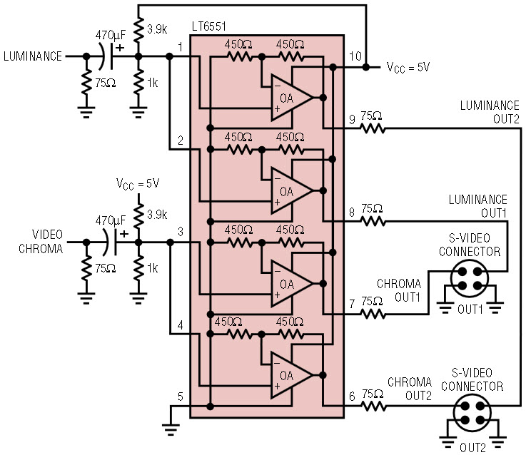
Figure 5. S-video splitter.
Buffered RGB to Color-Difference Matrix
High performance consumer products require generation of YPbPr luminance and chrominance component signals, often from standard RGB source content. The YPbPr format has a luma signal and two weighted color difference signals at baseband. Even with their fixed internal gain resistors, two LT6550s connected as shown in Figure 6 easily implement the required conversion matrix equations (also shown in Figure 6). To perform the conversion, the input to the Y channel of the second LT6550 is a simple weighted sum of the 2× amplified RGB signals from the first LT6550, creating a signal of 2Y. The Y channel output in the second LT6550 is fed back to its feedback resistor common pin. This configuration implicitly performs the required Y subtraction function for both of the color difference channels and sets the Y channel output stage to the required unity gain.
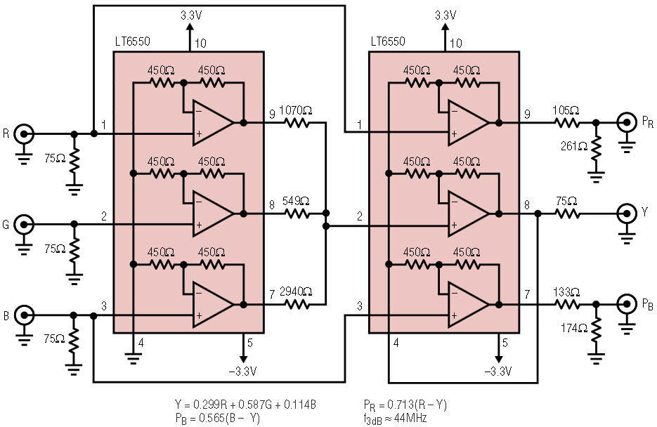
Figure 6. Buffered RGB to color-difference matrix.
The necessary scaling of the color-difference signals is performed passively by their respective output termination resistor networks. Since this circuit naturally produces bi-polar color difference signals (±0.35V at the cable load), the simplest implementation is to power the circuit with ±3.3V split supplies. With an available output swing of about 5.6V for this supply configuration, the circuit handles video with composite syncs and various DC offsets without difficulty. Since the Y channel normally needs to incorporate sync, either all of the RGB signals can have sync included or a 1.8mA gated current-sink can be introduced to the Y signal summing node to add sync.
Conclusion
The LT6550 and LT6551 triple and quad voltage feedback amplifiers are well suited for use in a variety of video applications. Their high slew rates, fast settling time, and wide input and output ranges make them an excellent choice for 3.3V RGB applications.


