
Redefining the Role of ADCs in Wireless
Today's wireless market is focused on moving as many components as possible from the analog domain to the digital domain to reduce cost per channel, size and power; improve reliability; and increase flexibility of the end product. To achieve these goals, the incoming signal at RF must be digitized, which would remove all analog components. However, existing technology is currently incapable of this method. The other, more practical method is to digitize the incoming signal after the signal has been mixed from RF to the first IF, which may range between 455 kHz and 250 MHz. This is commonly referred to as IF sampling if sampling removes the necessary second mix down stage from IF to baseband. The downconverted signal may not be just one RF carrier, but an entire band opening up the opportunity for software defined radio (currently under consideration by the FCC), an area that could potentially benefit high RF carrier count applications, such as cellular infrastructure.
With advances in high-speed, high-precision analog to digital converters, IF sampling is now possible. However, the performance requirements for the ADC must now take on the entire burden of the dynamic range that was once spread across many more components. This article concentrates on the necessary performance requirements of the ADC in current IF sampling receiver designs and how that performance can be achieved.
IF sampling
IF sampling is the process of sampling signals that are not at baseband, i.e., not centered around DC. Depending on the system involved, IF frequencies can be up to several hundred megahertz. Current ADC technology allows sampling of these frequencies with each generation of converters providing improvements in performance.
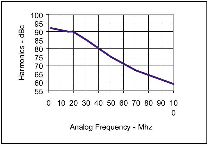
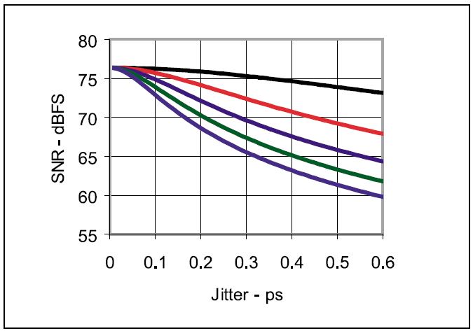
In general, converter performance begins to degrade with increasing input frequency. There are two primary areas of performance limitations. Within the converter, performance is limited by the slew rate of the on chip analog circuitry. Analog slew rate limitations result in a reduced SFDR performance as the input frequency is increased (see Figure 1). The other limitation to IF sampling is jitter on the sample clock. Although this limitation is due to external factors, it results in reduced SNR performance as the input frequency is increased (see Figure 2).
Different Nyquist zones
From a converter point of view, performance is divided into Nyquist zones. Nyquist states that the sample rate must be at least twice the signal bandwidth in order to faithfully represent the signal when sampled. With this in mind, an ADC has many different analog input ranges that can be used to satisfy Nyquist. The most common is the first Nyquist zone, which goes from DC to one half of the clock rate. Any signal or group of signals residing wholly within this range when sampled meets the Nyquist criterion. However, the same is true for signals that reside between one half of the clock rate and the clock rate. This is called the second Nyquist zone. This pattern continues for each multiple of one half of the clock rate.
A unique and useful effect of using the higher Nyquist zones is that signals sampled in the higher zones are mirrored down to the first Nyquist zone once digitized, thus forming the basis of a mixer and a digitizer, as shown in Figure 3.
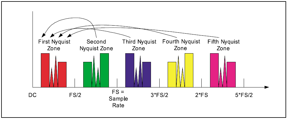
In addition to downconverting the sampled spectrum, signals placed in even Nyquist zones become spectrally inverted. Although this is usually not a problem, it can be useful to reverse a previously inverted spectrum as may occur in the first mixer.
High-speed clock rates
Fast encode clocks offer the advantage of making analog filtering significantly easier. Given a fixed signal bandwidth, a higher encode rate increases the allowable transition band. This will allow lower order filters to be used to reduce cost, or, if higher order filters are still used, greater stop band rejection can potentially be realized (see Figure 4).
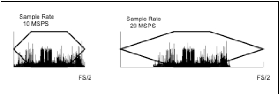
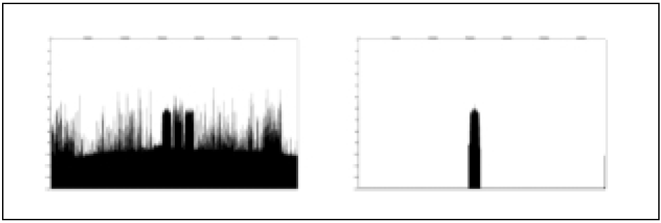
Another advantage with increasing clock speeds is processing gain. Processing gain is achieved when the signal of interest is oversampled and then digitally filtered (see Figure 5). Processing gain occurs when noise outside the band of interest is digitally removed, which results in improved SNR.
Processing gain can be easily determined using Equation (1). This equation determines the increase in SNR over and above the SNR of the converter alone.
ADC performance requirements
Two of the most important performance requirements to consider are the noise contribution and the spurious free dynamic range of the ADC. Before discussing how to optimize each in a receiver design, we will describe the theoretical noise power limit.
Traditionally, receivers are designed for maximum power transfer where the output impedance matches the input impedance of the following stage. Beginning at the antenna of the system, it can be seen that the noise voltage across the matched input terminals is
where k is Boltzmann's constant (1.38 × 10⁻²³j/K), T is temperature in K (~300 for room temperature), R is resistance, and Bw is bandwidth.
Available noise power from the antenna is therefore:
Combining these equations and solving for Pa yields
In a matched system, the noise power from the antenna is independent of the characteristic impedance. This demonstrates that KT is the fundamental noise floor of the receiver. Solving Equation (5) for a 1 hertz bandwidth gives −173.8 dBm/Hz.
If Equation (5) is solved at the antenna for the full Nyquist bandwidth of a 65 MSPS ADC (such as the AD6644, at 32.5 MHz), then Pa = 13.4 × 10⁻¹² watts. If Pa is then converted to dBm, it becomes −98.7 dBm at the antenna.
As the incoming signal moves through the receiver signal chain leading up to the ADC, two things must be considered. First, how is this theoretical number affected by the different cellular standards? Second, how is the signal affected by the gain and noise of subsequent stages of the receiver?
For a narrowband standard like GSM, which has 200 kHz bandwidth, substituting in Equation (5), the available noise power becomes −120.8 dBm due to channel filtering. For a multicarrier GSM system, such as the PCS band in the United States, the bandwidth may be as high as 15 MHz. Therefore, the available noise power is −102 dBm.
The other consideration is how the amplifiers and mixers of the receive signal chain (SC) contribute to the overall noise of the system. The noise presented at the antenna must be gained up by conversion gain and degraded by noise figure. If conversion gain is 25 dB and noise figure is 5 dB, the noise presented to the ADC in a 200 kHz bandwidth is:
or −120.8 dBm + 25 dB + 5 dB = −90.8 dBm.
Now that the noise for the rest of the receiver has been calculated, we will look at the noise contribution of the ADC. Unlike amplifiers, which are noise power devices, ADCs are voltage devices. For this reason, it is easier to analyze ADCs as voltage devices and then convert the results back to dBm. Consider, for example, a 14 bit 65 MSPS ADC, such as the AD6644. This ADC has a 2.2 volt peak to peak input range and a typical SNR of 74.5 dB.
or 21.42 × 10⁻⁹ volts2. This voltage represents all noises within the ADC, thermal and quantization. Converting volts to dBm yields −69.7 dBm (assuming 200 ohm input impedance into the ADC). Using Equation (7) for the processing gain of a 200 kHz channel, the effective SNR is improved to −91.8 dBm for the ADC.
The overall system noise can be determined by combining the front-end noise of the receiver and the ADC noise. The easiest way to combine these numbers is to convert back to power (in watts) and then add them together. The analog front end has 831.764 × 10⁻¹⁵ watts of noise and the ADC has 660.69 × 10⁻¹⁵ watts of noise, for a total noise power of 1.49 × 10⁻¹² watts. The other term that is necessary to compute the SNR is the fullscale input power of the ADC. If the fullscale input power is +4.8 dBm or 3.01 × 10⁻³ watts, then the maximum SNR in a 200 kHz bandwidth is:
or −93.05 dB.
To meet the minimum bit error rate (BER) requirements for a digital receiver, an SNR of ~5 dB must be maintained through the ADC. To calculate the minimum sensitivity at the antenna, we will look at the input of the ADC. To preserve the 5 dB of SNR, the input to the ADC would need to be at least −88 dBm. Normalizing for the full-scale input range of +4.8 dBm for the ADC, the input becomes −83 dBm. Subtracting 25 dB for receiver gain yields an input referred sensitivity at the antenna of −108.2 dBm.
Clock jitter
Since the noise requirements placed on the ADC are quite high, many things can limit the noise performance in a system. Clock jitter is one of the sample-to-sample variations in the clock source. Figure 6 shows jitter.
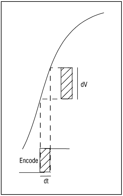
In Figure 6, the maximum slew rate is at the zero crossing of the sinusoidal input signal. When the clock samples at this point and there is jitter in the clock source, then an error voltage is generated. This error voltage degrades the noise performance of the ADC. As the ADC is moved up the signal chain to sample higher IF frequencies, the demands on the clock source become even greater, because the slew rate of the incoming signal increases with frequency and generates a greater error voltage. The amount of voltage error that is generated by clock jitter, as it relates to slew rate, can be solved using Equation (9):
To see how clock jitter affects SNR as a function of analog frequency, Equation (10) can be used.
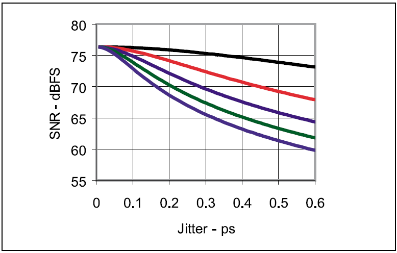
Using Equation (10), a family of curves that show the effects of clock jitter across several analog frequencies for a 14-bit ADC can be generated.
The two most common sources of clock jitter relate to the clock source itself and the buffer that is commonly used between the clock and the ADC. In order to achieve the best possible performance, a high quality clock source must be selected. Currently, the cleanest clock sources available are based on quartz crystal and offer less than 0.2 pS of jitter. Figure 7 shows that SNR is far better at high analog frequencies when using 0.2 pS of jitter versus 0.6 pS that is commonly used in high-quality synthesizers.
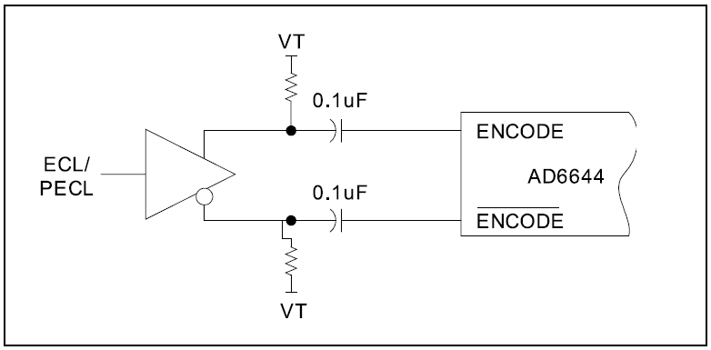
The other common source of clock jitter is the buffer between the clock source and the ADC. If a low jitter clock is available, one option is to AC-couple a differential ECL/PECL signal to the encode input pins, as shown in Figure 8. The advantage of using an ECL/PECL driver is that it has fast, slew rate matched outputs. One such device is the Motorola's MC100LVEL16.
Spurious free dynamic range
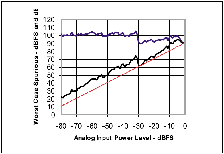
Like SNR, spurious free dynamic range (SFDR) helps determine the overall sensitivity of the receiver design. For an ADC, SFDR is defined as the ratio between the rms amplitude of a single tone and the rms amplitude of the worst spur as the tone is swept through the entire ADC input range. The specification that relates to SFDR is carrier to interferer ratio (C/I). The carrier is the desired signal and the interferer is either a carrier in an adjacent cellular band or a carrier that falls in band. If an interferer is sufficiently large, it may generate a spur that appears as a co-channel interferer of the desired signal, potentially blocking the desired call.
For example, assume an ADC has −90 dBFS of SFDR, as shown in Figure 9, and the required C/I is 18 dB. Normalizing the SFDR to the full scale (+4.8 dBm) of the ADC yields −85 dBm. In order to maintain the C/I ratio, the minimum signal that can be present at the ADC is −67 dBm (−85 + 18 dB). Translating back to the antenna and assuming 25 dB of gain yields a minimum sensitivity of −92 dBm. If the desired signal is smaller than this, the call may be blocked.
Dither
Because the SFDR requirements for narrowband air standards are so demanding, it is desirable to achieve the best possible SFDR from the ADC. One technique that is used to improve SFDR is dither.
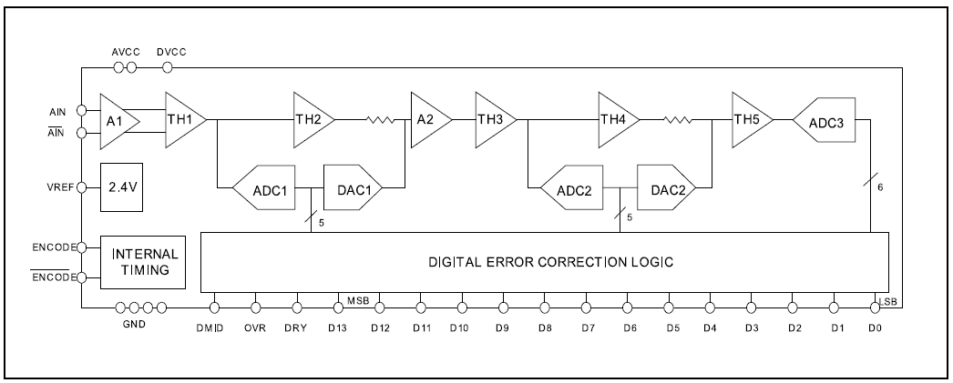
Dither is pseudo random noise injected into the analog input of the converter. To understand how dither improves SFDR performance, we must understand what generates distortion within the ADC itself. In a multi-stage ADC, for instance, the AD6644, there are two common sources for distortion: the slew rate limitation of the first track and hold, and the DNL errors in the transfer function of the ADC. Dither will improve the DNL errors but will have little influence on the track and hold errors.
The AD6644 is an example of how track and hold errors degrade SFDR. As shown in Figure 1, SFDR degrades dramatically beyond an analog input of 32.5 MHz. This degradation is a direct result of the slew rate limitation in the first track-and-hold. No matter how much dither is applied, the SFDR will not be improved at analog frequencies above this point.
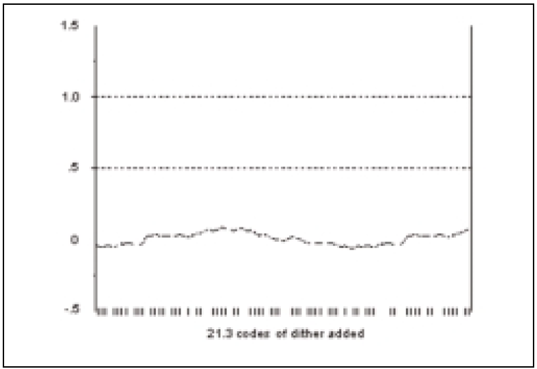
Within the AD6644, three stages are used to digitize the incoming signal. Because the last two stages are used repeatedly, the DNL error is repeated many times. The repeat count will be 2N where N is the number of bits in the first ADC. Dither randomizes the repeated DNL errors; thus, all codes appear uniform. An example of an ADC with DNL errors and how dither randomizes these errors is shown in Figure 10.
Many methods are available to implement dither, but the key is to maximize the benefit to SFDR while minimizing the impact on SNR. SNR can also be negatively affected because dither involves adding random noise into the analog path. To calculate the necessary dither, one must again look at the number of stages within the ADC itself. An ADC, such as the AD6644, has three separate stages; however, the most effective way in this case is to consider it as a two-stage ADC, where the first 5-bit ADC (front end) represents the first stage and the combination of the last two stages represents a single 9-bit ADC. (Two of the total eleven bits are error correction bits and should not count when applying dither.)
The last two stages can be combined because the effect of dithering the last stages independently is minimal, while the effect of dithering the last two stages together produces the most benefit. The 9-bit backend ADC stage will repeat every 512 codes. To ensure that the transition errors are completely randomized, enough dither should be added to dither across two repeat zones or 1024 p-p codes. To convert the p-p codes to dBm, we use Equation (11).
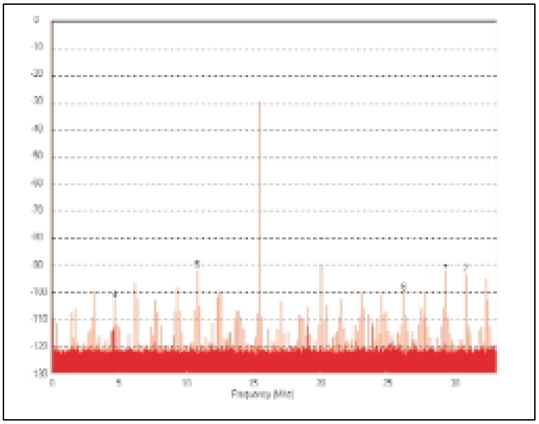
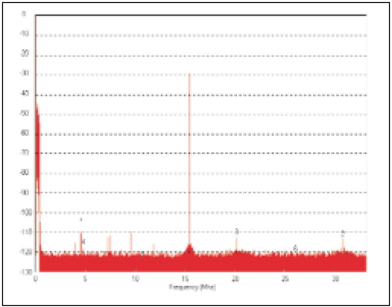
If Equation (11) is solved, −19 dBm of dither noise will provide the optimal SFDR while limiting the impact on SNR. Figures 12 and 13 demonstrate the effect of adding −19 dBm of dither.
Third order intercept point
Third order intercept point (OIP3) is not a specification normally associated with an ADC. Third order intercept point is usually used in reference to the power handling capabilities of a linear device, such as an amplifier with a given input and output impedance. An ADC is not a voltage input device and does not involve the transfer of power. However, this specification is very important when designing a receiver and often is needed to compute spurious response of a receiver.
For data converters, two-tone intermodulation is normally provided. The test is performed by stimulating the data converter with two different signals (usually unmodulated carriers) that are just less than one half scale. Since quantization within data converters limits the linearity, they do not exhibit the usual decrease in intermodulation when the input stimulus is reduced.
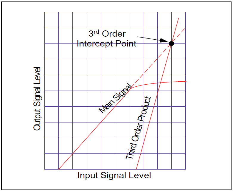
By comparison, typical linear devices, such as amplifiers, follow the relationship that the third order product increase and decrease at a rate that is 3 times faster than the input stimulus. Therefore, if the inputs are reduced by 1 dB, then the third order terms will be reduced by 3 dB. (This is based on the Taylor series representation of the nonlinearities of a linear device.)
Although OIP3 is usually based on the intersection of two lines (as shown in Figure 14), an approximation can be made for data converters using two-tone intermodulation data using Equation (12).
To use Equation (12), only the fullscale of the data converter in dBm (can be determined by the fullscale voltage and the load impedance) and the two-tone performance need to be known. For example, the AD6644 has a fullscale input power of +4.8 dBm (into 200 ohms) and gives −100 dBFS two-tone intermodulation performance. Using Equation (12), and then referencing to the fullscale of the converter gives
Therefore, the third order intercept (ADC input referred) is +54.8 dBm when referenced to the fullscale power of the data converter. Although this is a useful computational number, it should be remembered that data converters do not behave as normal linear devices.
Conclusion
Data converters have continuously improved over the last few years. Today's IF sampling converters offer the potential to simplify receiver architectures and, at the same time, allow greater flexibility. However, data converters are being considered more and more as RF devices. Traditional RF specifications, such as NF and IP3, are just as applicable to an ADC as they are to a mixer or amplifier.
Both SNR and SFDR will continue to be important in the future. Even the best data converters available still have a wide margin between actual performance and theoretical expectations. Therefore, the trend over the next few years may well be for better and faster converters of the same precision before additional bits are added.