Low Quiescent Current Surge Stopper: Robust Automotive Supply Protection for ISO 7637-2 and ISO 16750-2 Compliance
Low Quiescent Current Surge Stopper: Robust Automotive Supply Protection for ISO 7637-2 and ISO 16750-2 Compliance
by
Dan Eddleman
2017-01-01
Automotive power supplies produce formidable transients that can readily destroy exposed onboard electronics. Over time, as electronics have proliferated in vehicles, automotive manufacturers have duly noted failures, compiling a rogues’ gallery of the responsible power supply transients. Manufacturers have independently created standards and test procedures in an effort to prevent sensitive electronics from falling prey to these events. Recently, though, automotive manufacturers have combined efforts with the International Organization for Standardization (ISO) to develop the ISO 7637-2 and ISO 16750-2 standards, which describe the possible transients and specify test methods to simulate them.
ISO 7637‑2 and ISO 16750‑2 Standards
ISO7637 is entitled “Road vehicles—Electrical disturbances from conduction and coupling” and is an electromagnetic compatibility (EMC) specification. This article addresses the second of the three parts of this document, ISO 7637-2 “Part 2: Electrical transient conduction along supply lines only.”
Although ISO 7637 is primarily an EMC specification, prior to 2011 it also included transients related to power supply quality. In 2011, those portions related to power supply quality and not EMC were moved to ISO 16750, “Road vehicles—Environmental conditions and testing for electrical and electronic equipment” in the second of five parts, “Part 2: Electrical Loads.”
While most manufacturers still maintain their own specifications and requirements rather than adopt ISO 7637-2 and ISO 16750-2 verbatim, there is a trend toward more closely conforming to the ISO standards, with manufacturer specifications following the international standards with minor variations.
ISO 7637-2 and ISO 16750-2 provide specifications for both 12V and 24V systems. For simplicity, this article only describes 12V specifications and presents a circuit for protecting electronics connected to an automotive 12V power supply.
Load Dump
Load dump is the most challenging of the power supply transients because of the substantial energy in the event. It occurs when the alternator is charging a battery, and the battery connection is lost.
Alternators without Internal Voltage Clamps
Originally, alternators in cars were unclamped and could produce extraordinarily large voltages during load dump, about 100V for 12V systems. Newer alternators are clamped internally to limit the maximum voltage to a lower value during load dump. Because older alternators, and some modern alternators, do not include internal clamps, the load dump specification in ISO 16750-2 is split into “Test A—without centralized load dump suppression” and “Test B—with centralized load dump suppression.”
Figure 1 shows a schematic of an alternator’s 3-phase stator windings and the 6-diode rectifier that converts the stator’s AC output to the DC that charges the battery. When the battery connection is lost, the resulting current flow is as shown in Figure 2. Without the battery to absorb the stator’s current, the output voltage surges to the very high voltages seen during unclamped load dump, as shown in Figure 3 from the ISO 16750-2 specification. This corresponds to the unclamped alternator scenario in “Test A—without centralized load dump suppression.”
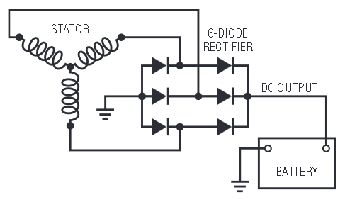
Figure 1. A standard alternator’s 3‑phase stator windings and 6‑diode rectifier produce a DC output voltage.
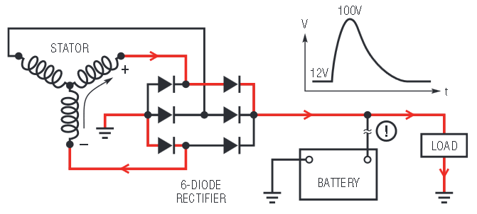
Figure 2. Unclamped load dump: If the battery connection is lost during charging, the alternator’s output voltage can surge to 100V.
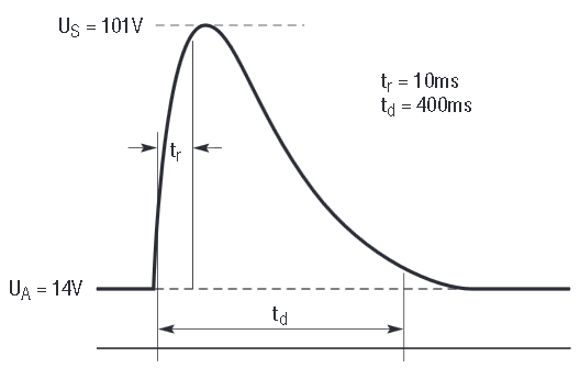
Figure 3. Unclamped load dump pulse shape as described in ISO 16750‑2 specification (“Test A...”).
Alternators with Internal Voltage Clamps
Newer alternators use avalanche diodes that have well specified reverse break-down voltages which limit the maximum voltage during load dump. Figure 4 shows current flow during a load dump fault in a clamped alternator that uses avalanche rated diodes in the six diode rectifier. When a clamped alternator is mandated by the automotive manufacturer, “Test B—with centralized load dump suppression” applies. Figure 5 shows the clamped waveform from Test B in ISO 16750-2. Although ISO 16750-2 specifies a 35V maximum voltage for this clamped scenario, be aware that many manufacturers deviate from ISO 16750-2 by providing their own maximum voltage specification.
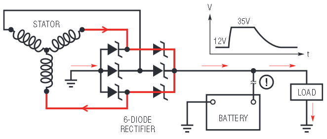
Figure 4. Clamped load dump: An internally clamped alternator has diodes with well specified reverse breakdown voltages that limit the output voltage to 35V during load dump.

Figure 5. Clamped alternator load dump pulse shape.
Also, be aware that when load dump was part of ISO 7637-2, only one pulse was specified, but when the load dump specification moved to ISO 16750-2 in 2011, the minimum test requirements increased to include multiple pulses with a one minute interval between pulses.
TVS Protection Problems
The internal resistance, Ri, of the alternator in both Test A and Test B is specified to be between 0.5Ω and 4Ω in ISO 16750-2. This limits the maximum energy that is delivered to protection circuits.
Nevertheless, one fact is frequently overlooked by those implementing protection from the ISO 16750-2 load dump transient: the internal resistance, Ri, does not appear in series with the 35V clamped voltage. Ri actually appears before the avalanche diode, as shown in Figure 6.
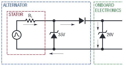
Figure 6. If the onboard electronics are protected by TVS diodes that break down at a lower voltage than the alternator’s clamped voltage, the TVS diodes will be forced to absorb all of the alternator’s energy.
If the onboard electronics are locally protected by a shunt device such as a TVS (transient voltage suppressor) diode with a breakdown voltage less than 35V, the TVS may be forced to absorb the alternator’s energy. In this scenario, the internal clamps in the alternator are of little benefit. The entire load dump energy is delivered to the TVS in the onboard electronics.
Sometimes a series resistor is placed in front of the electronics and the TVS diode, but unfortunately this introduces a voltage drop and extra power dissipation in the resistor even during normal operation.
ISO 16750-2 Requirements
While load dump is typically the most demanding condition described in ISO 16750-2, there are many additional requirements.
Reverse Battery
Section 4.7 of ISO 16750-2 describes “Reversed Voltage” or what most automotive engineers simply refer to as “Reverse Battery.” As you would expect, this specification covers the human error scenario where someone connects a battery with the polarity reversed. Obviously, this can result in destruction unless adequate protection is provided.
ISO 16750-2 requires that a 14V reverse test voltage be applied at all inputs for 60 seconds to ensure that the system survives without any damage. An alternative test condition of 4V reverse voltage is also allowed by ISO 16750-2 if no fuse is present in series with the alternator and the alternator’s rectifier diodes limit the voltage by conducting the substantial current delivered by the reverse connected battery.
Minimum and Maximum Supply Voltages
The minimum and maximum supply voltages are specified in section 4.2 “Direct current supply voltage.” The maximum supply voltage for 12V systems is 16V, and the minimum is as low as 6V. For hardware that is not capable of operating as low as 6V, other “codes” are assigned in ISO 16750-2 to classify the minimum operating voltage of the device. For this requirement, the equipment is expected to operate continuously.
Overvoltage
Section 4.3 of ISO 16750-2 describes “Overvoltage” requirements. The first requirement simulates the condition where the voltage regulator has failed. In this test, 18V is applied for 60 minutes. Depending on the application, it might not be necessary for the equipment to operate normally while the test is performed, but it must return to normal operation after the test condition is removed. The second test condition simulates a jump-start with 24V applied for 60 seconds. Once again, it may not be necessary for the equipment to operate normally during the test.
Superimposed Alternating Voltage
Section 4.4.2 provides test conditions to “simulate a residual alternating current on the direct current supply.” A peak to peak AC voltage of 1V, 2V, or 4V (specified as a “severity level”) is swept from 50Hz to 25kHz multiple times. The upper peaks of the voltage are at 16V and the series impedance is between 50mΩ and 100mΩ.
Supply Dips
Sections 4.5 and 4.6 of ISO 16750-2 address conditions where the input supply dips, either due to the battery discharging, another device in the automobile failing and blowing a fuse, or when the starter causes the supply voltage to dip.
Section 4.5 “Slow decrease and increase of supply voltage” simulates a battery being slowly discharged and then recharged. The supply voltage is discharged to 0V over a matter of minutes, and is then slowly brought back up. Obviously, it is not necessary to operate continuously, but this test verifies that the hardware does not fail in a destructive manner, and that it operates normally when power is restored.
In contrast, Section 4.6 “Discontinuities in supply voltage” is a much faster condition that attempts to simulate a failure in another circuit that causes the supply to dip until the other circuit’s fuse blows open. In this scenario, the supply dips to 4.5V for 100ms and then recovers with a rise time and fall time faster than 10ms.
The next part of Section 4.6 specifies a series of 5-second supply dips, with each pulse at a lower voltage than the previous one. The purpose is to verify that the device resets properly following a supply dip.
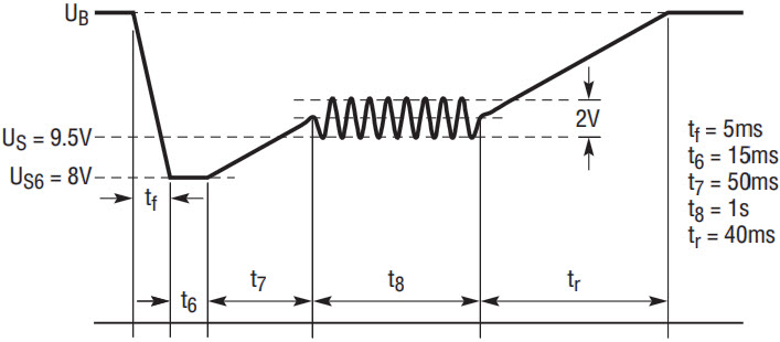
The third and last part of Section 4.6 specifies a waveform representative of a vehicle’s starting profile. It is applied to the device being tested 10 times. The exact voltages and durations required depend on the desired Level I, II, III or IV, which is determined by the application. The limits of Level I are shown in the figure below.
Open Circuit and Short-circuit Protection
Section 4.9 covers “line interruption” tests and describes procedures to ensure that a device resumes normal operation after connection is removed and then restored. Section 4.10 describes “short-circuit protection” tests and requires connecting each input and output to the maximum supply voltage and ground for 60 seconds.
Advantages of Active Protection With a Surge Stopper
A better solution is to use a series active protection device, such as the LTC4380 low quiescent current surge stopper. The LTC4380 block diagram is shown in Figure 7. A complete automotive protection solution is shown in Figure 8.
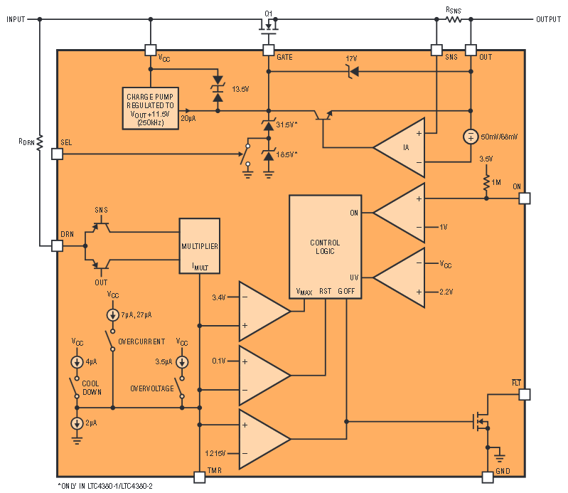
Figure 7. Block diagram of the LTC4380 surge stopper.
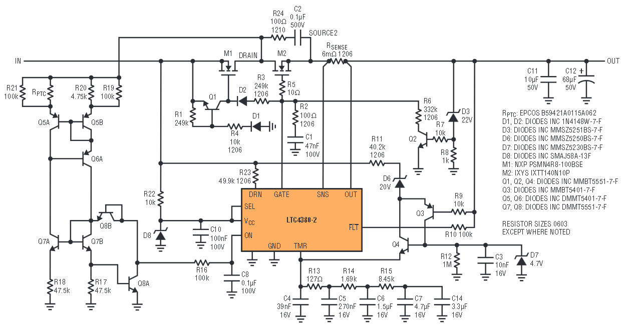
Figure 8. An LTC4380-based circuit protects downstream electronics from ISO 16750-2 and ISO 7637-2 transients while providing up to 4A of output current.
By its very nature, a surge stopper protects the downstream electronics from load dump as well as the other conditions in ISO 16750-2 and ISO 7637-2 without relying on the internal resistance of the alternator. The surge stopper solution shown in Figure 8 provides uninterrupted power while operating from a clamped alternator. Furthermore, if it is subjected to load dump from an unclamped alternator, it will not be damaged. In the unclamped scenario, it may shut off to protect itself and then automatically reapply power to the load after a cool-down period. It is important to note that power is only shut off in the presence of multiple simultaneous faults: an improper unclamped alternator is installed and the battery connection is lost during charging.
ISO 7637-2 Requirements
While the power quality portions of ISO 7637-2 moved to ISO 16750-2 in 2011, pulses 1, 2a, 2b, 3a, and 3b are still contained in ISO 7637-2.
Pulse 1
Pulse 1 describes the negative transient observed by electronics connected in parallel with an inductive load when the connection to the power supply is interrupted. Pulse 1 begins with the supply voltage collapsing to 0V as the supply voltage is removed. Soon thereafter, a −150V pulse is applied with a 2ms decay time. The energy of the negative pulse is limited by the 10Ω series resistance.

Pulse 2a
Pulse 2a describes the positive voltage spike that may occur when current is interrupted to a circuit in parallel with the electronics being tested. If current is built up in the wiring harness, when a device suddenly stops sinking current, the energy stored in the wiring harness inductance may cause a voltage spike. The energy of this positive spike is limited by a 2Ω series resistance.

Pulse 2b
Pulse 2b defines a situation that occurs when the ignition is switched off and DC motors act as generators. For example, if the heater is running when the driver turns off the car, for a short time the blower motor can supply DC power to the system while it spins down.
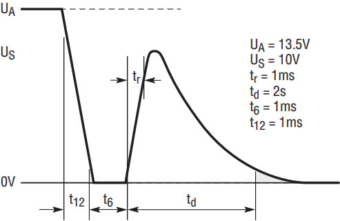
Pulses 3a and 3b
Pulses 3a and 3b are the negative and positive spikes that may occur as a result of switching processes including arcing across switches and relays. For this specification, the energy is limited by a 50Ω series resistance.
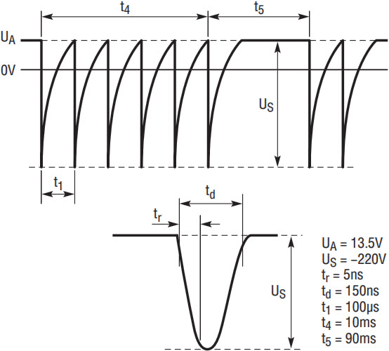
Pulse 3a figures.

Pulse 3b figures.
Operation of the Surge Stopper Protection Solution
The design in Figure 8 protects down-stream electronics from ISO 16750-2 and ISO 7637-2 transients while providing up to 4A of output current. At the same time, it protects the upstream system from over-current events caused by conditions such as short-circuit faults in the downstream electronics. As it does this, it consumes a miserly 35μA of quiescent current, an important consideration in modern auto-mobiles featuring countless battery-draining loads while the vehicle is not running.
This protection solution is based on the LTC4380 low supply current surge stopper, limiting the output voltage to 22.7V from input voltages as high as 100V at the input—sufficient protection against an ISO-16750-2 load dump as well as ISO 7637-2 pulses 1, 2a, 2b, 3a, and 3b. It also prevents current flow during reverse battery conditions, and provides continuous power during the ISO 16750-2 superimposed alternating voltage test at severity level 1 where the peak-to-peak AC voltage is 1V. (It may temporarily shut off power in the presence of larger AC volt-ages.) Continuous power is provided to the load when the input voltage drops as low as 4V to satisfy the minimum supply voltage requirements of ISO 16750-2.
The MOSFETs in this circuit are protected by limiting the time spent in high power dissipation conditions, such as when the input voltage surges high during load dump or when the output is shorted to ground. If a fault exceeds the conditions specified in ISO 16750-2 and ISO 7637-2, MOSFET M2 shuts off to protect the circuit, reapply-ing power after an appropriate delay.
For example, a sustained 100V input voltage, or a downstream short-circuit fault causes the surge stopper to self-protect by limiting the current in M2 and then completely shutting off if the fault persists.This method has a distinct advantage over shunt-type protection, which must dissipate continuous power—blowing fuses in the best case; lighting fires in the worst.
Load Dump and Overvoltage Protection
To understand the operation of the circuit in Figure 8, consider a simplified description of the LTC4380. During normal operation, the LTC4380’s internal charge pump drives the GATE pin to enhance M2. The voltage at GATE is clamped to a maximum of 35V above ground (when the SEL = 0V), thereby limiting the output voltage at M2’s source to less than 35V.
The circuit in Figure 8 further improves on that voltage limit by adding a 22V avalanche diode D3, in combination with R6, R7, R8, and 2 to regulate the output voltage to a maximum of the avalanche diode voltage, 22V, plus the base-emitter voltage of Q2, roughly 0.7V. When the output voltage exceeds 22V + 0.7V = 22.7V, Q2 weakly pulls down on M2’s GATE to regulate M2’s source and the output voltage at 22.7V.
Reverse Protection
MOSFET M1, in conjunction with D1, D2, R1, R3, R4, and Q1, protects the circuit from reverse voltage conditions. When the input falls below ground, Q1 pulls M1’s gate down to the negative input voltage, keeping the MOSFET off. This prevents reverse current flow when the battery is connected backward and protects the output from the negative input voltages.
D2 and R3 allow the LTC4380’s internal charge pump to enhance M1 during normal operation when the input is positive so that M1 is effectively a simple pass-through device, dissipating less than I2R = (4A)2 • 4.1mΩ = 66mW of power in the NXP PSMN4R8-100BSE.
SOA Limit
When the input voltage is high, the output voltage of this circuit is limited to a safe level by controlling MOSFET M2. This results in significant power dissipation as voltage is dropped across M2 while current is delivered to the load at the output.
If the input is subjected to a sustained overvoltage condition, or an overcurrent fault condition occurs in the onboard electronics at the circuit’s output, M2 is protected by shutting off after a duration configured by the timer network made up of R13, R14, R15, C4, C5, C6, and C14. The output current at the LTC4380’s TMR pin is proportional to the voltage across MOSFET M2 while M2 is in current limit.
Effectively, the TMR current is proportional to the power dissipated in MOSFET M2. The resistor/capacitor network at the TMR pin is similar to an electrical model of the MOSFET’s transient thermal impedance. This serves to limit the maximum temperature rise of the MOSFET to keep it within its rated safe operating area.
Because allowable MOSFET SOA current falls off at high drain-to-source voltages, the 20V avalanche diode D6, in conjunction with R9, R11, and Q3 provides extra current into the timer network when the IN-to-OUT voltage exceeds 20V plus Q3’s base-emitter voltage.The 4.7V avalanche diode D7 works with Q4, R12, and C3 to prevent this extra current from pulling the TMR pin above its maximum rated voltage of 5V.
This SOA tracking circuit allows the output to remain safely powered when the input rises to a high voltage. But, if a sustained high power fault condition lasts too long, the circuit self-protects by shutting off M2.
Thermal Protection
The resistor/capacitor network on the LTC4380’s TMR pin protects against events that are faster than about one second. For slower events, the case temperature of M2 is limited by the circuit connected to the LTC4380’s ON pin.
The thermistor, RPTC, is a small surface mount 0402-size component with a resistance of 4.7k at 115°C. Above 115°C, its resistance rises exponentially with temperature. To prevent the timer network from falsely integrating offsets in the power multiplier, the LTC4380 does not generate timer current at the TMR pin until M2’s drain-to-source voltage reaches 0.7V. With 4A and 0.7V, the MOSFET could dissipate 0.7V • 4A = 2.8W continuously without the TMR network detecting the MOSFET’s temperature rise. The PTC resistor, RPTC, in conjunction with resistors R17–R21 and transistors Q5A, Q5B, Q6A, Q7A, and Q7B shuts down the circuit if MOSFET M2’s case temperature exceeds 115°C.
Do not be dismayed by the number of components in the thermal protection circuit. The overall solution is relatively easy to implement and consists of small components that consume little board area. It is a self-biased circuit that is balanced when RPTC equals R20’s 4.75kΩ value. When the temperature of RPTC, which is placed in close proximity to M2, exceeds 115°C, its resistance grows and causes more current to flow through Q5B than Q5A. Because that results in more current through R17 than R18, Q8A’s base voltage rises and Q8A’s collector pulls the ON pin of the LTC4380 low, turning off M2. At lower temperatures, Q5A’s current is greater than Q5B’s, and Q8A remains off, allowing the ON pin’s internal pull-up to keep the ON pin high. Note that the ON pin current is used as the start-up current of this self-biased circuit through the diode-connected device Q8B.
Conclusion
The ISO 16750-2 and ISO 7637-2 specifications describe the challenging electrical transients that can occur in automotive systems. The LTC4380 low quiescent current surge stopper can be used to protect the onboard electronics from these transients, including both the clamped and unclamped load dump pulses. The circuit presented in this article provides uninterrupted operation when faced with load dump pulses from a modern, clamped alternator. When faced with more extreme unclamped load dump pulses, it shuts off to protect the down-stream electronics. The result is a robust solution for ISO 16750-2 and ISO 7637-2 compliance for electronics that draw up to 4 amps of supply current.
关于作者
Dan Eddleman是一名模拟工程师,在凌力尔特工作超过15年,曾担任过IC设计人员、新加坡IC设计中心经理和应用工程师。
他的职业生涯始于凌力尔特,设计了LTC2923和LTC2925电源跟踪控制器、LTC4355高压双通道理想二极管OR和LTC1546多协议收发器。他还是世界首款以太网供电控制器LTC4255的设计团队成员。他拥有两项与这些产品相关的专利。
随后,他搬到新加坡管理凌...
他的职业生涯始于凌力尔特,设计了LTC2923和LTC2925电源跟踪控制器、LTC4355高压双通道理想二极管OR和LTC1546多协议收发器。他还是世界首款以太网供电控制器LTC4255的设计团队成员。他拥有两项与这些产品相关的专利。
随后,他搬到新加坡管理凌...


