In-situ nonlinear calibration of a RF signal chain
Abstract
A new approach to linearize the cascade combination signal ICs, correcting in-situ for PCB imperfections and mutual loading is n of multiple RF/mixed proposed. This allows to substantially reduce system design/prototyping cycles and to maximize the signal chain performance at a negligible power consumption cost. Experimental results performed with RF signals up to 3GHz and using a 12b/10GSPS ADC are reported, validating the effectiveness of the approach.
Keywords—linearization, calibration, system design, analog-to-digital converter, digital-to-analog converter.
Introduction
Advancements in infrastructure communication systems, instrumentation and aero-defense applications drive ever higher performance requirements for RF and mixed-signal ICs, notably high speed / high dynamic range data converters [1-3].
Yet, printed circuit board (PCB) and packages, interposed between ICs in a signal chain, introduce parasitics and suffer of manufacturing imperfections leading to circuit imbalance in the network and compromising linearity of GHz signals.
An on-chip buffer is routinely present, in front of the track-and-hold amplifier (THA) of an analog-to-digital converter (ADC) to ease the coupling with an off-chip driving amplifier (or a variable gain amplifier). On-chip buffering ability is finite, power hungry and it weakens at high frequency. Mutual loading between ICs introduces additional non-linearity or alters the conditions in which ICs operate best.
A receive (Rx) signal chain is depicted in Figure 1. Each functional block (mixer, driving amplifier, filter and ADC; the latter including a front-end buffer and a THA) is a separate IC on the same PCB. While each block may perform optimally in isolation (or on the optimal custom board of a lab), once coupled and subjected to the strays and the limitations of a real-life PCB, the net performance of the overall chain can be limited.

Figure. 1. Example of a classic “receive” (Rx) signal chain.
Efforts are made by IC designers to strengthen the circuitry at the chip interfaces, to meet the required performance over a broad range of loading conditions. It is common that the system designers using the components need to customize and iterate a design in order to minimize the impact of the above described impairments. That effort is exacerbated by limitations in the IC’s high level models (often simplistic spreadsheets) and inadequate board stray modeling. Prototyping work can add several months to the development of a high performance system and require involvement from the application engineering staff of the IC suppliers [4, 5].
The nonlinear calibration (NLC) approach here introduced mitigates these problems by correcting dynamic nonlinear distortion over a wide range of input frequencies. The parameters for a nonlinear model of the overall signal chain of RF/mixed-signal ICs are determined in-situ, namely on the system board. A digital inverse corrective function nulling the second and third order distortion is then derived. This is performed in the foreground, before the signal chain processes signals. The inverse function is then applied, in real-time, to the data stream at the output of the ADC, hence post-distorting (linearizing) the effects of the impairments. This is reminiscent of digital pre-distortion (DPD) or of echo/transmit cancellation in communication systems [6].
This paper is organized as follows. Section II discusses the calibration system and its operation. Section III introduces the models adopted for the nonlinearity, the identification of the model parameters and the cancellation of the second and third harmonic distortion. Finally Section IV reports experimental results quantifying the effectiveness of the proposed calibration.
Nonlinear Cancellation for Signal Chains
Background
Let us assume that each of the ICs in Figure 1 (e.g. driving amplifier, filter, ADC) has already been individually optimized. So, for example, if the ADC requires internal foreground calibration [3], then that is completed beforehand.
Let us then consider the net static nonlinear characteristic existing, for example, between the ADC’s digital output Dout and the driving amplifier’s analog input vin as depicted in Figure 2. A cartoon curve (exaggerated for explanation’s sake) for that is sketched in the lower part of Figure 2. This captures the overall nonlinearity resulting from a variety of impairments, such as the residual imbalance between paired traces carrying differential analog signals between the amplifier and the anti-aliasing filter and between the filter and the ADC’s inputs, plus all the strays, plus the mutual loading between blocks etc.
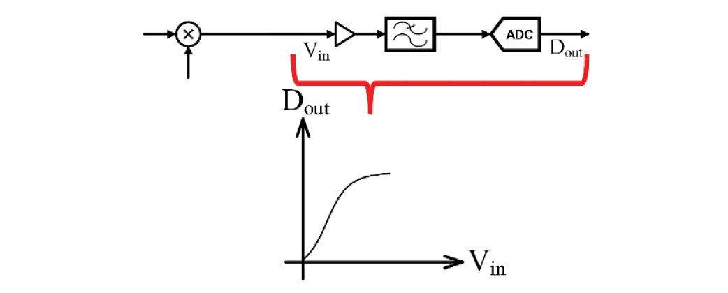
Figure. 2. Signal chain nonlinearity.
To appreciate this let us consider that, for example, the low frequency linearity of the ADC alone, is often better than 75dB, namely better than 1 part in 5000. Any board design imperfection or random manufacturing deficiency that is not significantly better than that will impact and degrade the net linearity of the signal chain, no matter what the ADC performance is. To make matters worse, in applications where wideband signals in the GHz range are processed, as in infrastructure communication systems or high performance instruments [6], this nonlinearity also has frequency dependent components and its behavior as such cannot be accurately modeled using only Taylor series expansion.
Operation of the algorithmic linearization
It is assumed that the signal path nonlinearity is a weak monotonic nonlinearity [6, 7]. Let H(.) be the model of the nonlinearity between Dout and vin as shown in Figure 2. The proposed approach to its cancellation consists in digitally inverting its distortion by applying an inverse function Hc(.) to the ADC’s output data stream Dout, returning a linearized data stream Dlin as sketched in Figure 3:

where G and D0 are the conversion gain and offset respectively. Hc(.) is embedded with the ADC as symbolized by the dashed line representing the converter chip.

Figure. 3. Digital correction for the nonlinearity. The inverse function Hc(.) is embedded with the ADC (the dashed line outlines the chip).
Hc(.) is characterized by a number of model parameters captured by the vector C. The following outlines the procedure to determine C in situ.
For that, H(.) needs to be exercised with an applied signal. This is done before the signal chain operates, without mixer output. A test signal u is generated and injected at the input of the driving amplifier. u is synthesized by a digital-to-analog converter (DAC) that is also on the same die with the ADC as in Figure 4, though integration is not a requirement. The DAC linearity needs to be superior to the target signal path linearity. A micro-controller uC is also embedded with the ADCin order to perform several functions, including the initial calibration of the ADCitself [3], and it is used here to control and perform the model identification algorithm and inverse function creation.

Figure. 4. Injection of the test signal.
The ADC output Dout corresponding to the digital representation of the signal u processed by H(.) is stored on an on-chip RAM. Following this, u is zeroed and the content of the RAM is processed by uC in order to estimate C, hence determining Hc(.,C) as shown in Figure 5 and elaborated on later.

Figure. 5. Determination of the correction parameters.
Once C is found, the signal chain is ready to operate with an actual vin, which is now the mixer’s output, and return a linearized output Dlin(since Hc(.) nulls the chain distortion). From this point on there is no change on C. Re-calibration is needed if the operating temperature or other parametric drifts have resurfaced excessive distortion [9].
The proposed approach is extensible to more functional blocks. For example, the mixer preceding the driving amplifier can also be included. For that the summing node for the injection of u moves upstream, on the left side of Figure 5, at the mixer’s signal input. The other mixer’s port needs to be excited with the local oscillator while u is applied but no other RF signal is applied to the mixer’s Rx input during this calibration phase. The procedure is conceptually the same as what has been previously described.
Modeling, Stimuli and Correction
Modeling
The adopted model type for both H(.) and its inverse Hc(.) is a parallel, time-discrete, Hammerstein model [8], consisting of parallel branches each containing a static nonlinear element followed by a dynamic linear element. This choice is justified by the nature of the dominant sources of the nonlinearity, which is, the continuous time driving amplifier, filters, buffer etc. [6, 7]. This is valid when other sources of nonlinearity, such as time-interleaving distortion or sampling charge injection distortion, have been previously made negligible [1-3, 9].
A complete dynamic model for the chain of Figure 5 is depicted in Figure 6. All blocks with a transfer function G are linear filters. For example, the ideal DAC output ucan be linearly frequency shaped by the transfer function Gdac, which, in general, may be different from the transfer function Gi from the mixer’s RF output. The model for H(.) consists of a linear component, a quadratic one and a cubic one, each one with their linear filters. The ideal quantizer Q returns the digital output Dout sampled at frequency fs.
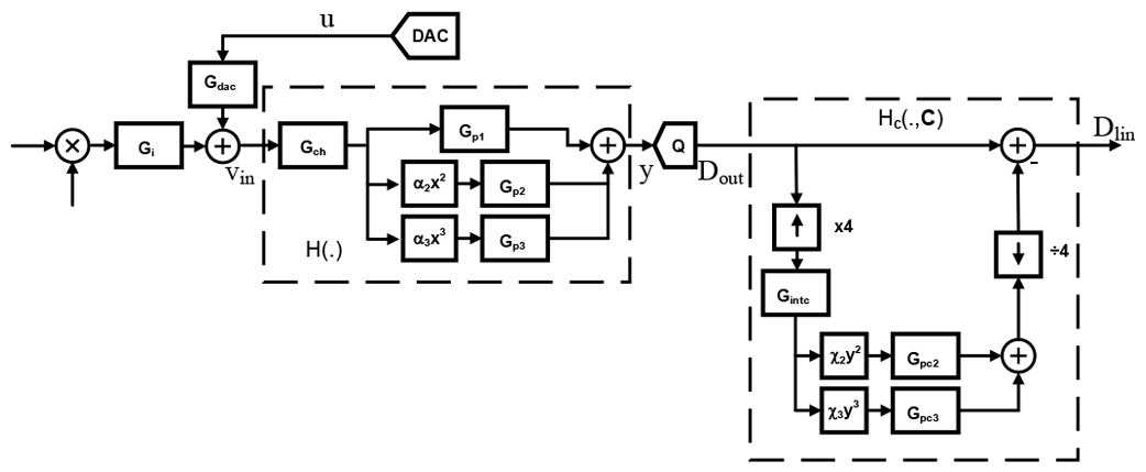
Figure 6. Full model for the chain, including H(.) and HC(.).
Dout is then processed by Hc(.,C), which too uses an Hammerstein model, where a quadratic component and a cubic component of the input signal are estimated, combined and subtracted from the distorted sequence Dout returning the corrected sequence Dlin. The coefficients of the functions in Hc(.,C) make up C and these can be directly algebraically related to those in H(.).
While vin is assumed to always be in first Nyquist band (the input frequency fin is assumed to be fin<fs/2), for high enough fin, its second and third order harmonics (at two and three times higher frequency respectively, hence these can end up in second and third Nyquist band) alias back to first Nyquist band after sampling by Q. This creates ambiguity in the correction function creation and, in turn, in the training algorithm for C and it also requires estimating the transfer function responses for the quadratic and cubic terms separately and up to the second and third Nyquist zones respectively. The ambiguity in correction has been resolved in HC by introducing a high enough interpolation, 4x in our case, before the genera-tion of the quadratic and cubic correction terms (subsequently decimated by 4 before applying the correction).
Stimuli and model identification
The DAC and the ADC are both clocking at rate fs. Both wideband pseudo-random sequences as well as single and dual tones have been used as stimuli to train the coefficients C and lead to comparable results though each of the two approaches has its own pros and cons. For the remainder of the paper, only the case of single tonal stimuli is discussed.
In this case, the DAC synthesizes u as a zero-order hold (ZOH) sequence of the form cos(ωt + ɸ0). Tones at multiple frequencies ω are generated, ensuring that the resulting harmonics don’t alias on top of each other (i.e. upon sampling, these do not fall in the same frequency bins).
With a simpler model for H(.) than what is shown in Figure 6, to keep math short, the distorted signal y(t) before the ideal sampler/quantizer Q can be written as y(t) = [α1vin(t) + α2vin2(t) + α3vin3(t)] *g3(t) where α2 and α3 are the distortion coefficients, and the nonlinear terms are convoluted with a linear time-invariant (LT I) impulse response g3(t). To correct Dout the training algorithm for Hc needs to estimate α2, α3, and g3(t).
The Fourier transform for y is:

where Г(ω) contains some other (cross-)terms not at ωo, 2ωo or 3ωo. This can be then written as:

where ɸ(ω) contains some other terms not at ωo, 2ωo or 3ωo and α’s and β’s can be related to one another. Since Dout is a digital representation of y, it follows that:

The fundamental, the second and the first harmonic resulting from H(.), scaled and phase shifted by G3 are readily visible. These terms map to the terms in Hc which cancel the quadratic and cubic terms. Hence C can be computed from H(.). In turn H(.) can be identified from its frequency response obtained by injecting tones u at evenly spaced frequencies, as explained in Section II, avoiding that the main harmonics fall on the same FFT bins. Then, as seen, C is algebraically found.
More algebra on (4) shows that when the second and third order harmonics of Dout alias into first Nyquist band, the corresponding terms in (4) are phase negated and this needs to be tracked. Also, rather than extracting β2G3(ejωo), β3G3(ej3ωo) in (4), their relationship to β1G3(ejωo) is actually used, hence requiring excitation only in first Nyquist zone but with more computation. If Gdac is a first order system, its impact can be accounted for by knowing the power of Dout’s fundamental. Finally, another practical limitation introduced by clocking the DAC at fs, as fin approaches Nyquist, is that u will be sinc-shaped, and, more importantly that u’s (fs – fin) first image also approaches Nyquist and creates spectral estimation issues.
Experimental Results
The NLC has been applied to a signal chain as in Figure 2 and using a chip, shown in Figure 7, embedding the 12b/10GSPS ADC described in [3], a 14b/10GSPS signal injection DAC, a 10GHz low phase noise clock synthesizer, the calibration engine (including the microcontroller uC) and other functions beyond the scope of this paper, such as a digital down converter and filters. The results reported here have been obtained for a sample rate of fs=6GSPS as required by a communication system with RF signals approaching 3GHz [6].
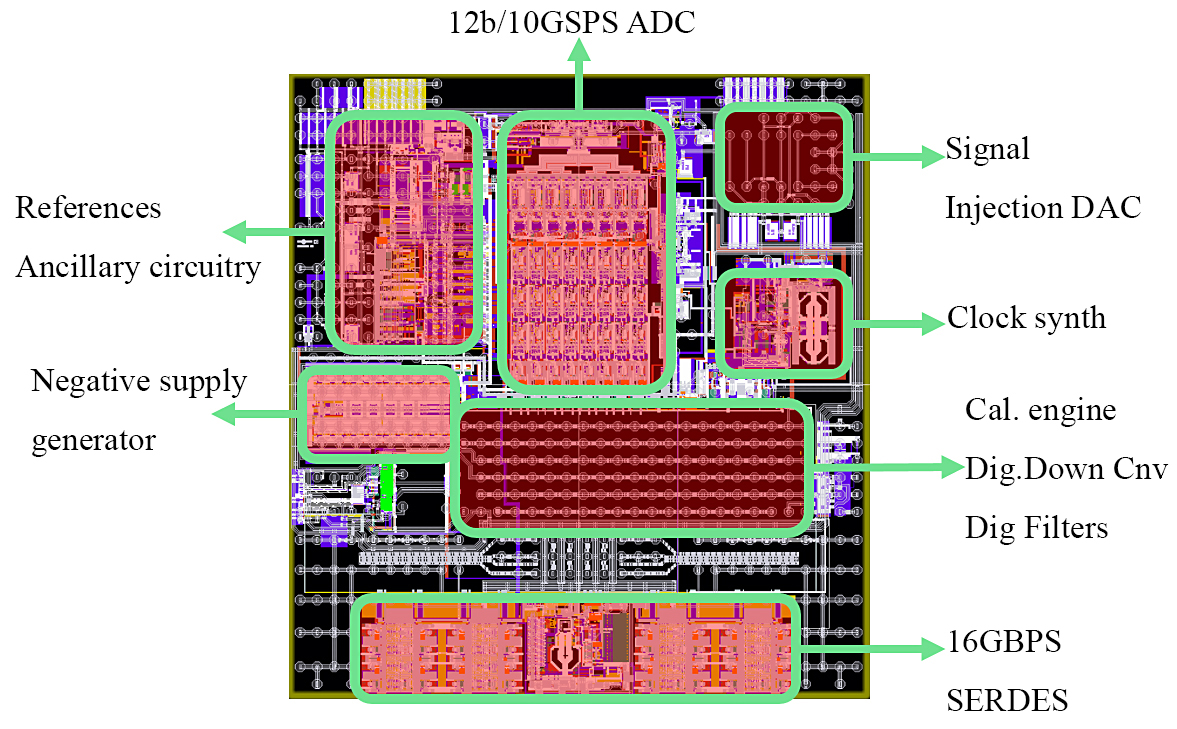
Figure. 7. Die layout and main functional blocks of the chip.
The single-tone second (HD2) and third harmonic (HD3) distortion performance, the signal-to-noise ratio (SNR), the spurious free dynamic range (SFDR) and the two-tones third order intermodulation distortion (IMD3) of the signal chain have been measured before linearization for near full-scale excitation. The results are reported in the curves marked as “nominal” depicted in Figure 8-11.

Figure. 8. Single tone distortion performance for (a) HD2 and (b) HD3 versus fin before linearization (nominal) and after linearization (corrected) for a fundamental input power of -1dBFS and fs=6GSPS.

Figure. 9. (a) SNR and (b) SFDR vs fin for an input at -1dBFS and fs=6GSPS.

Figure. 10. Two-tone IMD3 for (a) (2Fa–Fb) and (b) (2Fb–Fa) vs fin = (Fa+Fb)/2 for inputs at –7dBFS and fs=6GSPS.

Figure. 11. (a) HD2 and (b) HD3 vs fin for small input at –10dBFS and fs = 6GSPS.
The NLC is then applied and the performance metrics are measured once again and are reported in the same figures in the overlaid curves marked as “NLC corrected”. After NLC, the linearity performance substantially improves across nearly the entire Nyquist range, eventually reaching diminishing return as the input approaches fs/2, as anticipated. Fig 10a shows no impact to the noise performance (SNR), as expected. The improvement in SFDR in Figure 10b confirms the dominant contribution of HD2 and HD3, validating the assumptions made on the choice of the model.
While these curves show the system performance for near full scale (-1dBFS)excitation, it is important to confirm that the NLC holds for smaller excitation. So, without re-calibrating but only reducing vin’s power, the distortion has been re-measured at lower input power levels (i.e. -3dBFS, -6dBFS, -10dBFS). Due to space limitations, only the more extreme case of -10 dBFS is reported in Figure11. While the nominal performance has improved upfront due to the smaller excitation, except for a small degradation of HD2 at low frequency, the NLC performance is either better than or comparable to the nominal one, confirming the robustness of the approach.
In the calibrated chain, operating in real time, the application of the digital inverse function only adds about 150mW of power consumption on top of the total of over 5W consumed by the overall signal chain without correction.
