How to Design High Order Filters with Stopband Notches Using the LTC1562 Operational Filter (Part 2)
How to Design High Order Filters with Stopband Notches Using the LTC1562 Operational Filter (Part 2)
1999-02-01
Read other articles in this series.
This is the second in a series of articles describing applications of the LTC1562 connected as a lowpass, highpass or bandpass filter with added stopband notches to increase selectivity. Part 1 (Linear Technology VIII:2, May 1998, pp. 28–31) described one method of coupling the four Operational Filter™ building blocks of the LTC1562 to design an 8th order lowpass filter with two stopband notches. Part 2 expands the technique of Part 1 to design an 8th order bandpass filter with two stopband notches.
Throughout this series of articles, notches will be generated by first summing the input signal with a 180 degree out-of-phase signal appearing at the output(s) of the LTC1562 Operational Filter and second, by adjusting the summation gains to yield a zero sum.
Part 1 showed one proprietary method of creating notches in the stopband of a lowpass filter. The essence of this method is briefly revisited in Figure 1, where two of four Operational Filter sections are coupled to form a 4th order lowpass filter with one stopband notch. The notch is obtained by summing the input signal, VIN, with the output, V1A, into the inverting node of the next section of the IC. The two signals, VIN and V1A, will tend to cancel each other at a frequency where they are 180 degrees out of phase. The cancellation will be complete if the amplitudes of VIN and VIA yield equal (and opposite) currents at the summing junction of the op amp of Figure 1, that is if:

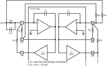
Figure 1. Two out of four Operational Filter sections are coupled to form a 4th order lowpass filter with one stopband notch.
In Figure 1, the lead capacitor CIN1 raises the frequency where a 180 degree phase shift occurs above the center frequency of the 2nd order section (fO). The resulting notch frequency is then higher than the cutoff frequency of the 4th order filter.
Figure 1 can be easily modified to make the frequency of the notch lower than the center frequency of the 2nd order section from which it is derived. This is useful in bandpass filters where an unwanted frequency lower than the center frequency of the filter must be rejected. This is shown in Figure 2, where the input signal is summed with output V2A instead of output V1A. The frequency of the resulting notch is:

and the gain conditions dictating Equation 1 now translate to:

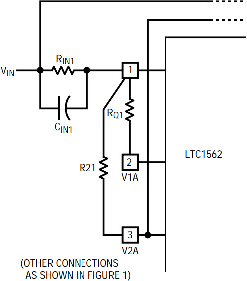
Figure 2. Figure 1’s circuit modified to make the frequency of the notch lower than the center frequency of the 2nd order section from which it is derived.
The circuit of Figure 2 can be used to build a 4th order bandpass filter with one notch below its center frequency. Such a filter can simultaneously detect a tone and reject an unwanted frequency located in the vicinity of the passband.
The notch techniques of Figures 1 and 2 will be referred as “feedforward.” This is necessary to separate these techniques from others to be shown later, in Part 3 of this series of articles.
The feedforward notch technique of Figure 2 can be advantageously combined with Figure 1 to realize sharp bandpass filters with two stopband notches: one notch below and one above the center frequency. Filters of this type can be very selective, although they are quite cumbersome to design. A step-by-step design procedure is illustrated below.
A Practical Example
An 8th order 100kHz bandpass filter is realized, through FilterCAD™ for Windows® (available at no charge from Linear Technology—see the “Design Tools” page in this issue), by cascading four 2nd order sections of equal Q. The –3dB band-edges are arithmetrically symmetric with respect to the filter’s 100kHz center frequency and signals below 80kHz and above 125kHz are attenuated by 60dB or more. Figure 3 shows the theoretical amplitude response and Table 1 shows the desired filter parameters, namely, the center frequencies, Qs and notch frequencies. The filter of Figure 3/Table 1 can be realized by decomposing the 8th order realization into two independent 4th order filter sections and then cascading these two 4th order sections, which is an easier task than designing an 8th order elliptic bandpass filter all at once. FilterCAD, in custom mode, should be used to perform this operation. Figure 4 and Table 2 show the filter decomposition and the cascading sequence; note the left and right notches. Figure 5 uses the LTC1562 Operational Filter to realize the filter of Figure 3 as decomposed in Figure 4. The design is split into two 4th order sections. The algorithm to calculate the external passive components is outlined below.
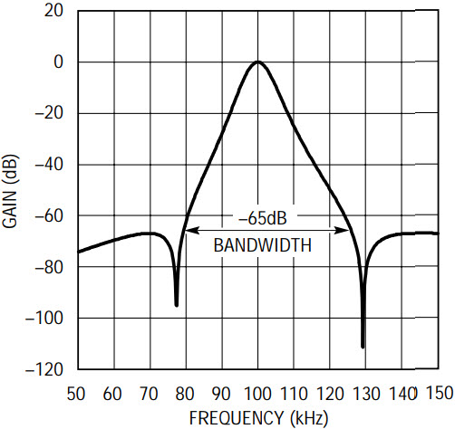
Figure 3. Theoretical amplitude response of 8th order, 100kHz bandpass filter.
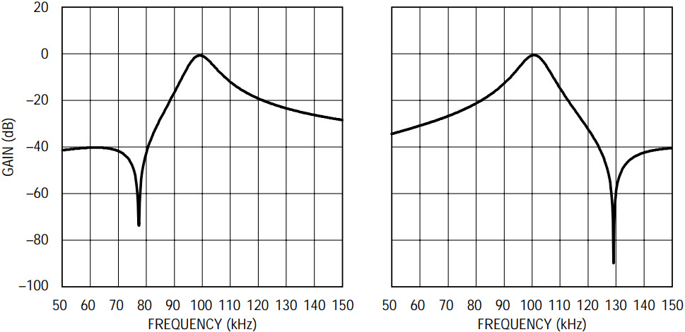
Figure 4. Cascading two 4th order bandpass sections to realize the filter of Figure 3.
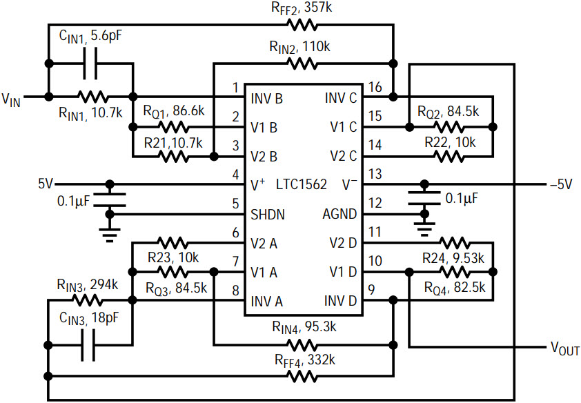
Figure 5. Hardware realization of the filter in Figure 3, using all four sections of an LTC1562.
| fO | Q | fN | QN | Type |
| 99.9687e3 | 10.0000 | — | — | PB |
| 96.9964e3 | 10.0000 | 129.2814e3 | — | LPN |
| 103.0322e3 | 10.0000 | 77.3023e3 | — | HPN |
| 100.0000e3 | 10.0000 | — | — | BP |
| fO1 = 96.9964k Q1 = 10 fO1 = 99.9687k Q2 = 10 fN2 = 77.3k H(s) = GAIN • N(s)/D(s) GAIN = 0.2823 N(s) = A1s(s2 + 235 • 9072 • 109) A1 = 62.8122 • 103 |
fO3 = 100k Q3 = 10 fO4 = 103.0322k Q4 = 10 fN2 = 129.2814k H(s) = GAIN • N(s)/D(s) GAIN = 0.1788 N(s) = A1s(s2 + 659 • 83 • 109) A1 = 62.8319 • 103 |
In order to obtain a practical realization that closely approximates the theoretical one, the Q of each 2nd order section will be lowered by 15%. (Please consult the LTC1562 final data sheet.)
In order to follow the long and tedious algorithm below, consider the intuitive outline: We need to calculate the following set of passive components for the first 4th order section: RIN1, CIN1, R21, RQ1, and RIN2, RFF2, R22 and RQ2. The resistors R21, RQ1, R22 and RQ2 are easily calculated via the expression for the center frequency, fOi, and Qi for the 2nd order section “i.” The expression for the notch, equation (2), involves the product of RIN1 • CIN1, so neither component can be calculated separately. Instead, RIN1 is calculated by considering the maximum gain (which occurs around the center frequency fO1) at either node V1A or V2A. This controls premature internal clipping. Once RIN1 is set, CIN1 is easily calculated via equation (2) for the lower band notch. Similarly, equation (3) defines the ratio of RIN2 to RFF2, so neither of these components can be calculated independently of the other. RFF2 is calculated by considering the gain factor (“GAIN”) of the 4th order filter section at the V1B output (Figure 1/Table 2)). Once RFF2 is set, RIN2 is calculated via equation (3).
The same design method is later repeated to derive the passive components for the second 4th order section:
I. Calculate the passive components of the of the first 4th order section (fO1 = 96.9964kHz, Q = 8.5, fO2 = 99.9687kHz, Q = 8.5, fn2 = 77.3kHz)
- Calculate the center frequency-setting resistor, R21: (For details, please refer to the LTC1562 data sheet.) R21 = (100kHz/fO1)2 • 10k = 10.629k (choose the closest 1% value, R21 = 10.7k (1%))
- Calculate the Q-setting resistor, RQ1: (For details, please refer to the LTC1562 data sheet) RQ1 = Q1 √R21 • 10k = 87.925k (choose the closest 1% value, RQ1 = 86.6k (1%))
- Calculate the input resistor RIN1 from the following expression(s):
- 3a. if fO1 ≤100kHz (for LTC1562)
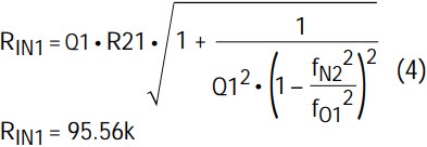
Although not applicable for this example, thoroughness dictates mentioning the case below:
- 3b. if fO1 ≥ 100kHz (for LTC1562)

Make sure, in either case 3a or 3b, that RIN1 is greater than R21, that is, the DC gain at pin 3 in Figure 5 is less than unity; if not set RIN1 = R21 and proceed to step 4a.
The expression for RIN1 sets the gain at fO1 equal to unity at the node of maximum swing (V1A or V2A). Note that, for high Qs, the gain at fO1 is the maximum gain. If you know the spectrum of the signals that will be applied to the filter input and if internal gains higher than unity will be allowed, the value of RIN1 can be reduced to improve the input signal-to-noise ratio.
- 4a. Use the value of RIN1, calculated above, and calculate the value for the input capacitor CIN1 from the notch equation (2).
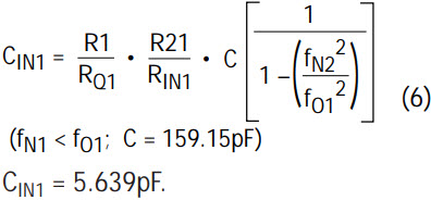
Use the commercially available NPO type 0402 surface mount capacitor with the value nearest the ideal value of CIN1 calculated above. For instance, for CIN1, choose an off-the-shelf 5.6pF capacitor.
- 4b. Recalculate the value of RIN1 after CIN1 is chosen. RIN1 = (CIN1(ideal) RIN1(ideal))/CIN1(NPO,0402) = 96.22k Choose the closest 1% value: RIN1 = 95.3k (1%)
- Calculate the frequency- and Q-setting resistors R22, RQ2, as done in steps 1 and 2, above. Choose the closest 1% standard resistor values. R22 = 10k (1%); RQ1 = 84.5k(1%)
- Calculate the feedforward resistor, RFF2: 1/(RFF2 C) = Gain • A1; C = 159.15pF
The values for parameter (Gain • A1) are provided by FilterCAD; they relate to the coefficients of the numerator of the transfer function (V1B/VIN in Figure 1); a passband AC gain of unity is assumed (see Table 2). Please note that, for a lowpass case, as in Part 1 of this article series, the value of (Gain • A1) is the DC gain of the filter and its value can be easily set without software assistance.
Equating the numerator of the filter transfer function with the values provided by FilterCAD:


- Solve for RIN2 by using Equation (3), which dictates the gain condition for the occurrence of the notch: RIN2 = (RFF2 RQ1 CIN1)/(R1 C) = 108.785k; (R1,C) = (10k, 159.15pF) RIN2 = 110k (1%)
II. Calculate the passive components of the second 4th order section (fO3 = 100kHz, Q3 = 8.5, fO4 = 103.0322kHz, Q4 = 8.5, fn4 = 129.2814kHz) Except for the bandpass gain calculations, the algorithm will be the same as the lowpass design of Part 1 of this article.
- R23 = (100kHz/fO3)2 • 10k = 10k (1%)
- RQ3 = Q3 √R23 • 10k = 85k, RQ3 = 84.5k (1%)
- Calculate the input resistor RIN3 from the following expression(s):
- 3a. if fO3 ≤ 100kHz (for LTC1562)

- 3b. if fO3 ≥ 100kHz (for LTC1562)

For fO3 = 100kHz, as in the example above, either expression can be used. Note that the expression for RIN3 in 3b, above, is the same as expression for RIN1 shown in Part 1 of this article.
- 4a. Use the theoretical value for RIN3, calculated above, and calculate the value of the input capacitor CIN3 from the notch equation (2) of part 1 of this article; for convenience this is repeated below:

Use a commercially available NPO-type 0402 surface mount capacitor with the value nearest the ideal value of CIN3 calculated above. For instance, CIN3 = 18pF.
- 4b. Recalculate the value for RIN3 calculated in step 3a after CIN3 is chosen.

- Calculate the frequency- and Q-setting resistors, R24 and RQ4, as done in steps 1 and 2, above. Choose the nearest 1% standard value.

- Calculate the feedforward resistor, RFF4. First equate the numerator of the 4th order filter transfer function with the values provided by FilterCAD (see Table 2):
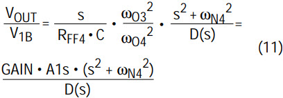


- Solve for RIN4 by using equation (1) of Part 1 of this article, which dictates the gain condition for the occurrence of a notch. For convenience, this gain condition is repeated below.

Experimental Results
Figure 6 shows the measured amplitude response of the filter of Figure 5. The values of the passive component are as calculated above and as shown in Figure 5. The measured amplitude response closely approximates the ideal response as synthesized by FilterCAD. The peak frequency with standard 1% resistor values and 5% capacitor values is 100.65kHz (0.65% off). The higher frequency notch, although it shows a respectable depth of 70dB, is not as well defined as the notch below the filter’s center frequency, yet the –65dB bandwidth is as predicted by FilterCAD. The 10dB lack of the upper band notch depth is due to the finite speed of the internal op amps; they cause the practical 180 degree phase shift frequency and the gain at V1A’s output to depart slightly from the theoretical calculations.
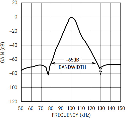
Figure 6. Measured amplitude response of Figure 5’s filter.
For the sake of perfection, the notch depth can be easily restored by tweaking the value of RQ3; the new RQ3 will be 75k. This is shown with dashed lines in Figure 6. This, however, lowers the passband gain by the ratio of the new to the old RQ3 value, that is, by about –1.0dB (you cannot fool mother nature). Depending on the application, the 10dB of additional notch depth for 1.5dB of passband gain loss may be a reasonable trade. The passband gain can also be corrected by lowering the values of either pair, (RFF2, RIN2) or (RFF4, RIN4), by the same amount (1.5dB). In Figure 6, the gain was restored to 0dB by changing the values of RIN2, RFF2 to 93.1k and 300.1k respectively.
The total integrated noise was an impressively low 69µVRMS, allowing a signal-to-noise ratio well in excess of 80dB. The input signal-to-noise ratio can be further increased if the passband gain can be higher than 0dB or if internal nodes are allowed to have gains higher than 0dB. Please contact the LTC Filter Design and Applications Group for further details.
The low noise behavior of the filter makes it useful in applications where the input signal has a wide voltage range. This is true provided the filter magnitude response does not change with varying input signal levels, that is, the filter gain is linear. The gain linearity measured at the 100kHz theoretical center frequency of the filter is shown in Figure 7. The gain is perfectly linear for input amplitudes up to 1.25VRMS (3.5VP-P) so an 84dB dynamic range can be claimed. The input signal, however, can reach amplitudes up to 3VRMS (8.4VP-P, 92dB SNR) with some reduction in gain linearity.
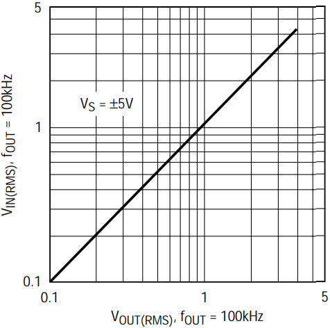
Figure 7. Gain linearity of Figure 5’s filter, measured at the 100kHz theoretical center frequency.


