Hot Swap for High Availability Systems
Introduction
Critical computer, mass storage and communication systems are designed to operate with zero down time, or to at least approach that ideal. Such high availability systems must continue functioning even when system upgrades and maintenance are performed. Often this requires circuit boards be inserted into, and removed from, a live powered system.
Hot swapping requires a power switch to initially isolate and then control inrush current via a controlled ramp up of power, which prevents any disturbance to the backplane and adjacent circuits. Because the Hot Swap circuit is the gateway for all board power, it is a natural place to monitor and collect power supply data. Such data reveals the health of the board and the integrity of the power path.
With this in mind, the LTC4260 combines a wide input range Hot Swap controller, ADC voltage monitor, I2C™ serial communication, and other features in one device (see Table 1). The LTC4260’s Hot Swap circuit uses an external N-channel pass transistor to isolate the hot swapped board from the backplane when it is first inserted. After a de-bounce time the controller can begin to apply power to the board or wait for a turn-on command from a host processor. Power is ramped gradually to minimize any backplane disturbance. After the power-up process is complete, the LTC4260 continues to monitor for faults in the power path.
| Feature | Benefits |
| Wide Input Voltage Range: Operates from inputs of 8.5V to 80V, with 100V absolute maximum | • Suitable for 12V, 24V and 48V systems • Simplifies design because part functions on a semi-regulated supply. • Large overvoltage transient range eases design tolerances for transient protection. |
| 8-Bit ADC: ADC monitors current, output voltage and external pin voltage and measures off-state current in the FET to determine FET failures | • Increases reliability. • Board power information provides an early warning of board failure. • Verify board is staying within its alloted power • Allows integrity check of redundant supply paths |
| I2C/SMBus: Communicates as a read-write slave device using a 2-wire serial interface. | • Improves integration with the host system. Interface allows the host to configure the part, determine which faults are present or have occurred, and read back ADC measurements |
| Fast Short Circuit Response: Fast (<1μs) current limit response to shorts | • Protects connector from overcurrent. • Limits the short circuit caused glitch on the input supply. |
| Alerts Host after Faults: When configured (using I2C), faults activate an active pull-down on the ALERT pin | • Interrupting the host for immediate fault servicing limits system damage. |
The LTC4260 provides the means for quantitatively measuring the board current and voltages with an onboard ADC and multiplexer. It reports this information using the I2C serial communication bus when polled by a host processor. The device will interrupt the host for specific fault conditions, if configured to do so.
The LTC4260 works in applications from 80V (with transients to 100V) to 12V battery systems where the operating range could drop to 8.5V.
An Inside Look
The block diagram of the LTC4260 is shown in Figure 1. The lower section of the block diagram shows the ADC voltage monitoring, the registers and the I2C interface.
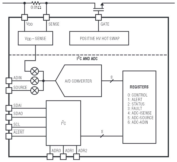
Figure 1. Block diagram of the LTC4260.
The ADC monitors the current via the sense resistor voltage, VDD-SENSE. The SOURCE pin and the external ADIN pin are also multiplexed to the ADC. The registers allow the user to configure the part and to read back useful information on the status of the part and if any faults have occurred.
The I2C block uses a 2-wire serial interface using the SCL and SDA signals. To facilitate communications across two isolated grounds, the SDA is split into SDAI and SDAO pins to allow the part to drive optoisolators with a minimum number of external components. For normal I2C communications sharing a common ground these two pins are shorted together.
The ALERT pin is used for interrupts. The upper block diagram contains the Hot Swap blocks required to monitor the input supply, and when appropriate to turn on the gate of the external pass transistor.
Measure Real-Time Board Power with Integrated ADC
Collecting and compiling information on the voltage and current flowing into each card is a useful way to measure the health of the card. Operating data can be compared to historical data to discern whether a card was actually using its allotted power or if it was operating abnormally. An abnormally operating card could be flagged for service, perhaps even before it failed. The LTC4260 includes an 8-bit data converter that continuously monitors three voltages: the ADIN pin, the SOURCE pin and the amplified difference between the VDD and the SENSE pins. The ADIN pin is an uncommitted ADC input. This pin allows the user to monitor any available voltages.
The ADIN pin is monitored with a 2.56V full scale direct connection to the converter. The SOURCE pin uses a 1/40 divider at the input which gives a 102.4V full scale. The VDD-SENSE voltage amplifier has a voltage gain of 33.33 which results in a 76.8mV full scale.
The results from each conversion are stored in three ADC registers (see Table 2) and updated 10 times a second. Setting the test mode control register bit halts the data converter so that registers can be written to and read from for software testing.
| Register | Description |
| CONTROL | Register turns-on or turns-off the pass transistor and controls whether the part will Auto-Retry or latchoff after a fault. It also configures the behavior of the GPIO pin |
| ALERT | Alert register enables which faults interrupt the host using the ALERT pin. At power-up the default is to not alert on faults. |
| STATUS | Status register provides pass transistor (on/off), BD_PRST (high/low) and GPIO (high/low) conditions. It also lists five fault present conditions. |
| FAULT | Fault register logs overcurrent, overvoltage, undervoltage, power-bad, FET short and BD_PRST changed state faults. |
| SENSE | ADC data for the VDD–SENSE voltage measurement |
| SOURCE | ADC data for the SOURCE pin voltage measurement |
| ADIN | ADC data for the ADIN pin voltage measurement |
Typical Hot Swap Application
An N-channel pass transistor Q1 in the power path, as shown in Figure 2, controls power to the board. The sense resistor RS detects current for overcurrent faults and ADC measurements. Capacitor C1 controls the GATE slew rate while resistor R6 compensates the current control loop. Resistor R5 suppresses self-oscillations in Q1. Resistors R1, R2 and R3 provide undervoltage and overvoltage sensing at the input while R7 and R8 provide output power-good monitoring.
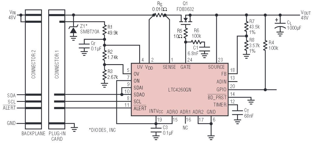
Figure 2. This 3A, 48V Hot Swap application resides on the plug-in card.
The staggered pins of the male connector ensure all power supplies are physically connected before output power is allowed to ramp. The following is a typical board insertion sequence:
- Long power and ground pins make contact and the internal 5.5V supply (INTVCC) becomes active. The internal registers are reset after a power-on-reset pulse. The pass-transistor (Q1) is off.
- The medium length pins, SDA, SCL and ALERT make contact. This allows I2C communication to begin.
- The short pin connects resistor R1 to the supply voltage bringing the UV and OV pins to the adjusted level. The UV, OV and BD_PRST pins must remain in the acceptable range for 100ms to ensure that any contact bounce during insertion has ended. After 100ms the ON pin is tied high. If it is high, then the external switch turns on. If it is low, the external switch turns on when the ON pin is brought high or if a serial bus turn-on command is received.
Power-Up Sequence
The pass transistor is turned on by charging up the GATE with a 18μA current source. The voltage at the GATE pin rises with a slope equal to 18μA/C1 and the supply inrush current is set at

When the GATE voltage reaches the Q1 thresholdt voltage, the switch begins to turn on and the SOURCE voltage follows the GATE voltage as it increases.
The LTC4260 uses 3.5V reference, a precision voltage comparator and an external resistive divider to monitor the output supply voltage. When the voltage at the FB pin rises above the 3.5V threshold, the GPIO pin, in its default configuration ceases to pull low, indicating that the power is now good. Figure 3 shows a typical Hot Swap, 100ms delay and power-up event.
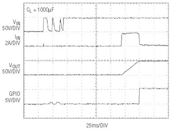
Figure 3. Power-up waveforms for the 48V Hot Swap application.
Controlled Turn-Off
Controlling the GATE pin slew rate during turn-off prevents inductor driven voltage spikes on the drain and source of the pass transistor due to the rapid change in current. The controlled turn-off of the switch uses a 1mA current pulling the GATE pin to ground. Normally the turn-off is initiated by the ON pin going low or a serial bus turn-off command. Additionally, several fault conditions will turn off the switch. These include an input overvoltage (OV pin), input undervoltage (UV pin), overcurrent circuit breaker (SENSE pin) or BD_PRST going high.
LTC4260 Resides on Either Side of the Connector
In Figure 2 the LTC4260 is located on the plug-in board side of the connector. The backplane side of the connector contains power and signal routing. Some designers choose to place the Hot Swap controller on the backplane or motherboard side of the connector along with host processing of the data.
A typical backplane resident application is shown in Figure 4. The plug-in card is inserted into an un-powered slot with ground and power pins mating first. Next the connection sensing pin directly ties the BD_PRST pin to ground. This signals the Hot Swap controller to begin a power-up sequence.
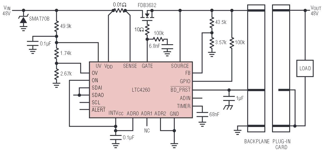
Figure 4. This 3A, 48V Hot Swap application resides on the backplane or motherboard.
If the LTC4260 shuts down due to a fault, it may be restarted by simply removing and reinserting the card. There is an internal 10μA pull-up current source on the BD_PRST pin. When the card is removed and re-inserted the BD_PRST pin is pulled high then low which clears the offending fault and begins a new power-up sequence.
Fast Current Limiting Isolates Faults and Protects Backplane Voltage
The LTC4260 features an adjustable current limit with foldback that protects against excessive power dissipation in the switch during active current limit. The current limit level is set by the value of the sense resistor located between the VDD pin and the SENSE pin. When the load current exceeds the current limit, the LTC4260 regulates the GATE pin voltage to keep the current through the sense resistor at a constant value.
The response time to an overcurrent depends on the sense voltage, as shown in Figure 5. In the case of a short circuit in the load, the current is brought under control in less than 1μs. The GATE pin is pulled down with a 600mA GATE-to-SOURCE current.
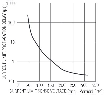
Figure 5. The response time to an overcurrent depends on the sense voltage. In the case of a short circuit in the load, the current is brought under control in less than 1μs.
To protect against excessive power dissipation in the switch, the current limit folds back or drops as a linear function of the output voltage, which is sensed at the FB pin. The current limit threshold as a function of output voltage is shown in Figure 6.
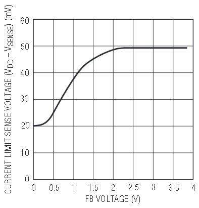
Figure 6. To protect against excessive power dissipation in the switch, the current limit folds back or drops as a linear function of the output voltage, which is sensed at the FB pin.
An overcurrent circuit breaker limits the time the part is in active current limit. While the LTC4260 is in active current limit the capacitor CT is charged with a 100μA pull-up current. If the voltage at the TIMER pin reaches 1.235V, the part turns off the pass transistor and records an overcurrent fault. Figure 7 shows output short waveforms.
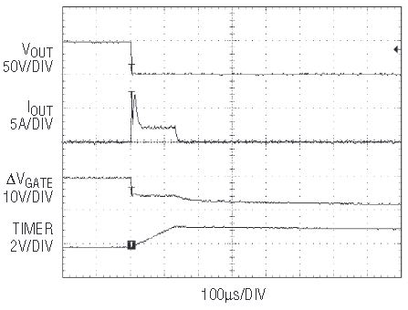
Figure 7. Short circuit waveforms.
Control Board Power through I2C Interface
The LTC4260 features seven registers as shown in Table 2. The control register sets the state of the pass transistor and controls whether the part automatically attempts to turn on after certain faults or stays in the latched off state.
One bit in the control register sets the ADC to test mode, where a host processor can write into the ADC registers. The mass write feature, which allows the use of a special I2C address to write to all LTC4260s at once, can be masked using a bit in the control register.
The control register also configures the behavior of the general purpose input/output (GPIO) pin. At power-up the GPIO pin defaults as a powergood indicator. Other uses for the GPIO pin are as a power-bad indicator, general logic input pin or a general logic output pin.
The alert register sets which faults interrupt the host. There are control bits for each specific fault allowing the ALERT pin to pull low when that fault occurs. At power-up the default state is to not alert on faults. After the bus master controller broadcasts the Alert Response Address, the LTC4260 responds with its address on the SDA line and releases ALERT.
Collecting Fault Information Aids Diagnosis
After a board fault occurs, diagnosing the problem is simplified by checking the LTC4260’s onboard fault information. The fault and status registers contain a record if faults are present or have occurred and can be accessed through the I2C interface.
Three major faults can turn off the pass transistor: overcurrent, undervoltage and overvoltage. An undervoltage fault occurs when the UV pin drops below 3.12V while an overvoltage fault occurs when the OV pin rises above 3.5V. Each of these major faults has an auto-retry control bit. If a fault occurs and its auto-retry bit is set, then once the fault is removed, the LTC4260 turns on the pass transistor. Otherwise the part is latched off until the fault register is cleared.
There are three minor faults recorded by the fault register that do not turn off the external FET. They include the power bad, BD_PRST changed state and FET short.
A power bad fault is reported if the FB pin drops below the 3.41V threshold while the FET is on. The board present feature allows detection when downstream cards are inserted or removed. This fault is labeled as BD_PRST changed state. The last minor fault, the FET short, indicates current is flowing in the sense resistor when the pass transistor is turned off. A FET short fault is reported if the data converter measures a current sense voltage greater than or equal to 2mV when the FET is off.
The Status register contains useful information regarding the FET’s on or off condition, all the major and minor fault present conditions and the logic level of the GPIO pin. The Fault register can be regarded as a running log of past faults.
Clearing the Fault Lets the Output Turn-On
As mentioned earlier, the overcurrent, undervoltage and overvoltage faults, once written into the fault register, will keep the pass-transistor off if auto-retry is not selected for these faults. This remains true even when the original recorded fault condition is no longer present. The fault register must be cleared to turn on the output. The fault register is cleared with any of the following ways:
- Writing zeroes into the fault register bits using I2C bus
- An ON pin high to low transition crossing the 1.235V threshold
- Writing a high-to-low transition in the FET on bit (control register)
- UV pin brought below 1.235V
- VDD brought below 7.45V
- INTVCC brought below 3.8V
- BD_PRST high-to-low transition crossing the 1.235V threshold clears all faults except BD_PRST changed state fault.
Conclusion
The LTC4260 is a smart power gateway for hot swappable circuits. It provides inrush control and fault isolation while it closely monitors the power through its gates. It logs faults and can interrupt the host if necessary, all while monitoring board power using an internal 8-bit ADC.
I2C is a trademark of Philips Electronics N.V


