High Accuracy Clock up to 170MHz in a SOT-23
Introduction
Crystal based oscillators are often the default choice for designers looking to clock today’s high speed microcontrollers, data converters and programmable logic devices. Crystal oscillators, although convenient, accurate and stable, come at a high price in use—they occupy considerable board space, consume significant power, and are sensitive to environmental factors like shock and temperature extremes. The LTC6905 is an all silicon clock that avoids these pitfalls, making it an alternative to crystal oscillators in applications up to 170MHz.
Accuracy and jitter specifications of the LTC6905 are more than sufficient for most applications, and its power and size advantages allow the LTC6905 to fit in designs where a crystal oscillator could never go.
Device Description
The LTC6905 is a part of Linear Technology’s line of resistor controlled SOT-23 oscillators. These resistor controlled oscillators use a single external resistor to accurately set the oscillator frequency, and there is a simple linear relationship between the resistor value and the frequency (see Figure 1). The LTC6905 is pin-compatible with the LTC1799 SOT-23 oscillator, but uses a different control resistor range and a different formula to set the frequency.
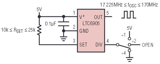
Figure 1. A single resistor sets the frequency of this tiny, robust oscillator.
The LTC6905 is also available in fixed frequency versions, where the resistor is internal to the part and no external components other than a bypass capacitor are required. Preset devices with master oscillator frequencies of 133MHz, 100MHz, 96MHz and 80 MHz and 1.5% accuracy are available. These devices have an internal divider which makes it possible to produce most popular frequencies between 20MHz and 133MHz. Devices can be customized to output any frequency in the range of 2.2MHz to 170Mhz.
The LTC6905 uses an internal feedback loop to accurately match the impedance of a switched capacitor element to the external resistor connected to the RSET pin, thus setting the master oscillator frequency. The voltage level on the DIV pin engages internal dividers to divide this master frequency by 1, 2 or 4 before it is sent to the OUT pin. With fixed frequency devices, the LTC6905-XXX series of parts, the RSET pin is replaced by an output enable pin, which disables the output when it is connected to GND.
The voltage on the RSET pin of the LTC6905 is forced to a bandgap controlled voltage of 1V below the positive supply, independent of the temperature or supply voltage, with a tolerance of less than 5%. This stable RSET voltage makes the LTC6905 ideal for applications where an accurate voltage or current controlled frequency is required.
The frequency range of the master oscillator in the LTC6905 is limited to between 70MHz and 170MHz, which corresponds to external frequency setting resistor values between 10kΩ and 25kΩ. This range is expanded by the internal dividers to between 17MHz and 170MHz, and is limited by the architecture of the high speed master oscillator.
The master oscillator of the LTC6905 is a voltage controlled ring oscillator, and provides a unique jitter profile where the jitter percentage remains relatively constant over frequency. Traditional relaxation oscillators develop a larger percentage jitter as the frequency increases. The jitter of the LTC6905 actually decreases with increasing operating frequency, making it ideal for high frequency applications.
Fixed Frequency Devices
The LTC6905 can be ordered in a fixed frequency version where the frequency-setting resistor is inside the part. An output enable pin is made available in place of the RSET pin on these devices only. Four versions are available: LTC6905-133, LTC6905-100, LTC6905-96 and LTC6905-80. These four versions collectively offer 12 popular frequencies through the use of their DIV pins. Please see Table 1.
| DIV Setting | LTC6905-133 | LTC6905-100 | LTC6905-96 | LTC6905-80 |
| V+ (÷1) | 133.33MHz | 100 MHz | 96 MHz | 80 MHz |
| OPEN (÷2) | 66.66MHz | 50MHz | 48MHz | 40MHz |
| GND (÷4) | 33.33MHz | 25MHz | 24MHz | 20MHz |
The LTC6905-XXX fixed frequency oscillators offer several advantages that stem from their internal resistor configuration. The parts are less sensitive to external noise that may couple into the RSET pin on the external resistor version of the part. This lack of sensitivity translates into improved jitter of less than 1% at all frequencies and accuracy of better than 1.5% over commercial temperature range. The internal resistor parts are generally more accurate because they are trimmed at one specific frequency and do not have any error term from nonlinearities over the RSET resistor range.
The absence of an RSET pin on the fixed-frequency devices has made room for an output enable pin. This output enable synchronously disables the output drivers when brought low, and does not produce pulse slivers. Power dissipation is significantly reduced because much of the power is dedicated to driving output capacitance. The internal master oscillator and bias networks remain active in order to facilitate an immediate and accurate frequency output when the output is enabled. If the output enable pin is left floating or pulled to the positive supply, the oscillator is enabled.
Layout Considerations
Because the LTC6905 combines a high frequency oscillator and output stage with a sensitive analog control loop, it is necessary to exercise great care in board layout to maximize accuracy and stability. The bypass capacitor must be placed as close as possible to the LTC6905, preferably on the same side of the board. Even the small inductance and resistance of vias in the pc board can adversely effect part performance. Additionally, the traces to the bypass capacitor should be larger than is indicated by the power consumption of the device. Although the average power consumption is low, driving a capacitively loaded output will induce spikes in the supply current which must be damped by the bypass capacitor.
The RSET pin is the most sensitive input pin, and attempts must be made to shield it from noise coupling or excessive parasitic capacitance. It is recommended that the frequency setting resistor be located as close as possible to the RSET pin, and that the frequency setting resistor be connected to the positive supply as close as possible to the V+ pin. A recommended layout is illustrated in Figure 2. If the bypass capacitor must be situated on the opposite side of the PC board from the LTC6905, it is strongly recommended that the connection between the capacitor and the LTC6905 be as short as possible and use multiple, filled vias to minimize series inductance and resistance.
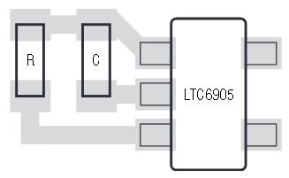
Figure 2. LTC6905 Suggested layout. Note that the bypass capacitor is located adjacent to the device and on the same side of the PC board.
The LTC6905 is specified at an output load of 5pF, which is equivalent to about two standard HC logic inputs. Driving this load at 170MHz is the single largest factor in the power consumption of the LTC6905. The power supply current needed to drive a capacitive load may be calculated as:

where CLOAD is the 5pF load capacitance, VSWING is the voltage swing, in this case up to 5.5V, and FOSC is the frequency of the oscillator. Driving a 5.5V swing into a 5pF load at 170MHz takes 4.675mA on average.
The majority of this power is expended during the risetime and falltime of the output signal, not while it is in a steady state. The 500ps rise and fall times of the LTC6905 mean that the instantaneous power supply current required during the rise and fall portions of the waveform is much greater than the average. The instantaneous power supply current may be calculated by a similar formula:

where trf is the rise/fall time of the signal. In this case, 55mA spikes are generated by driving 5.5V into a 5pF load.
Because of these power supply spikes, and because of the tendency for fast edges to couple into adjacent lines, the layout of the output trace is critical. Capacitance, trace length and loading should be minimized. Additionally, with traces longer than a few centimeters, transmission line effects must be taken into consideration.
Should output loading and coupling problems occur, there are methods to mitigate the effects. A series resistance in the range of 50Ω–1000Ω placed adjacent to the output pin of the device will increase the rise and fall times of the signal being driven into the output load, and therefore reduce power supply spikes and coupling (see Figure 3). A 50Ω cable may be driven using a 950Ω series resistance and a 50Ω termination to ground, though the signal will be attenuated (see Figure 4). A high speed comparator or inexpensive AHC series CMOS logic gate may be placed in the signal path directly after the LTC6905 in order to buffer the output signal and drive heavier loads.
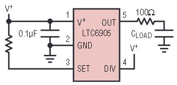
Figure 3. A series resistor on the LTC6905 output pin reduces power supply spikes caused by load capacitance.
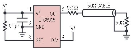
Figure 4. The LTC6905 can drive a 50Ω cable with appropriate termination.
Voltage and Current Controlled Oscillators
The LTC6905 is an ideal candidate for making a voltage or current controlled oscillator. Unlike other resistor controlled parts, where the voltage on RSET varies with power supply and temperature, the LTC6905 maintains the voltage at the RSET pin at 1V below the positive supply. Because the frequency of oscillation is based on the resistance, or V/I at the RSET pin, a stable V at the RSET pin provides the ability to generate an accurate output frequency by injecting an accurate current (I) at the RSET pin.
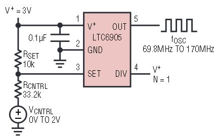
Figure 5. The LTC6905 as a voltage controlled oscillator.
For stability reasons, it is recommended that the RSET pin be driven by resistors as shown in Figure 5. All modulation of the frequency, whether by voltage or current, relies on modulation of the current input to the RSET pin. Because the RSET voltage is fixed at 1V, the frequency of the output depends to the first degree only on the current into the RSET pin. The master oscillator frequency may be approximated as:

Substituting VRSET/IRSET for RSET, where VRSET=1V, we get:

This indicates that a 50μA current into the RSET pin would result in a master oscillator frequency of 85MHz. More applications circuits and information regarding using the LTC6905 as a VCO is available in the data sheet.
The modulation bandwidth of the LTC6905 is dictated by its internal control loop, which is limited to between 700kHz and 2MHz, depending on output frequency. Due to the low modulation bandwidth in relation to the output frequency, it is recommended that the LTC6905 be used as a VCO only in applications where the rate of modulation is less than the output frequency divided by 128.
Conclusion
The LTC6905 and LTC6905-XXX are low power, highly accurate silicon oscillators that can replace crystals in many applications. They offer advantages of lower cost, lower sensitivity to temperature and shock, and ease of frequency modulation—important features in driving microcontrollers, FPGAs and other complex systems.


