Complying with Latchup Qualification Requirements in High-Voltage Power Analog ICs
摘要
High-voltage (HV) power analog integrated circuits (ICs) are used in most every electronic system, including battery power conversion, audio, automotive, industrial, medical, and LED drivers. Ensuring that the design of such ICs complies with latchup qualification requirements involves a conceptually different approach compared to designing with digital LV ICs. This application provides guidance on analog IC design for latchup compliance.A similar version of this application note originally appeared on EDN on April 18, 2018.
Introduction
The design considerations for ensuring that high-voltage (HV) power analog ICs comply with latch-up qualification requirements are rather different when compared to the approach used to design digital low-voltage (LV) ICs. The LV IC’s electrostatic discharge (ESD) and latch-up design challenges are typically addressed at the level of I/O library cells that can be re-used in various products without customization.The HV ICs usually combine several voltage domains isolated from p-substrate. From a cost perspective, junction-isolated process technologies are dominant. They support so-called isolation N-pockets to enclose the devices and circuit blocks. In an extended CMOS (ECMOS) process, the pocket is formed by a set of deep Nwell (DNW) implants. Because of the limits of deep implantation, this approach achieves a pocket voltage rating within a 40V range. A voltage range up to 120V can be achieved using a bipolar CMOS DMOS (BCD) process technology, where the N-pockets are formed by a combination of buried layers, optional sinkers, and a relatively thick, grown N-epitaxial layer. This technology integrates power-optimized complementary lateral DMOS devices with drain extension and either non-self-aligned or double diffusion scheme for source and body regions1. The minimum process layout design rules for the pocket isolation are inadequate for a latch-up injection test. Instead, application-specific latch-up design rules for a complex layout are needed.
Overall, latch-up design rules, standards, and checker descriptions infrequently explain the reasoning behind their methodological steps in conjunction with real design. Such an understanding often helps to organize the practical experience to be effective. In this application note, we address the gap in understanding of such a diverse, novel, and complex subject as HV analog IC design from the latch-up prospective. We connect, in a logical order, the explanation on the semiconductor structure level followed by the introduction of injector-victim formalism for latch-up collection features and prevention spacing rules. Then, we apply a set of definitions to the experimental methodology for latch-up-spacing rule parameters and block-level verification principles toward the practical concept of the IC-latch-up co-design. Rather than delivering a broad review of the HV latch-up subject, either from a historical or diversity prospective, this application note presents a successfully verified-by-practice approach.
The latch-up is a side-effect of parasitic structures formed by the regions of integrated active devices. At the proximity of certain regions, the injected carriers can diffuse and drift long distances in substrate and, at a certain current level, initiate a non-linear conductivity modulation due to positive feedback between impact ionization, thermal carrier generation, and the parasitic bipolar gain. As a result, a temporary electrical state deviation can induce a non-dedicated strong-current path. It can further result in irreversible damage or formation of a conductive state that cannot self-dissipate as long as the original power supply state remains unchanged (i.e., latch-up). The latch-up state is usually detected by comparing the power-supply currents before and after the stimulus.
The latch-up states can be induced either by current injection from a forward-biased junction connected to I/O pins or by an overvoltage of power-supply pins during the test pulse. In a real environment, the effect can be caused by power surges, electromagnetic interference (EMI) events, intermittent connection with an inductive load, hot plug-in, and ionizing radiation. The latch-up robustness is essentially an IC quality measure that represents an ability to withstand a certain level of the short-term electrical state deviation and return to the original functional state without irreversible changes. Respectively, the qualification test according to the standard2 emulates two events: the current injection in the I/O pins and the overvoltage of power-supply pins. Typical criterion is less than 10% change of all power-supply currents and passing of a full functional test program.
Thus, the latch-up test essentially examines the stability of a particular IC design against relatively short-term deviations of the operation conditions of the pins interfacing with the environment. An analogy of a similar-purpose test for ESD conditions is the power-on mode system-level ESD test[3,4]. Due to the lack of coverage by conventional circuit simulation models, the pass level of the latch-up test is hard to predict without a dedicated approach.
Understanding HV Latch-Up
HV IC latch-up arises both for the overvoltage and injection latch-up test modes. The maximum operating voltage (MOV) and absolute maximum voltage rating (AMR) are the two main ratings related to elevated voltage levels. Operation within the MOV range guarantees long-term reliability, while increasing the voltage above the AMR can cause an immediate irreversible failure. Respectively, for the range between MOV and AMR, a survivability is expected and, namely in this state, the latch-up test is accomplished. The uncertainty is related to the correlation between the formal data sheet IC pin AMR voltage, which can be set as low as 10% over MOV, real physical AMR of the integrated devices connected to the pin, and real physical AMR of the IC pin with a particular layout design.
Propagated from LV digital ICs, the standard overvoltage test for the supply pin is defined up to the level of 1.5 x MOV2. The same level limits the voltage compliance for the injection current test if the current limit is not achieved. While this voltage level can be easily met in LV CMOS circuits, the HV circuits with power-optimized LDMOS do not always tolerate it. A way around this is the approach of maximum stress voltage (MSV), which limits the test voltage2. The injection test induces the detection current between the HV pins, which can lead to high Joule heating.
However, the main instance of the HV latch-up is related to the parasitic structures themselves. The easiest way to explain this is through a comparison with a more familiar LV latch-up. The LV latch-up typically involves the current path through the parasitic silicon-controlled rectifier (SCR) formed either inside the I/O cell or in the core circuit.
For example, in the push-pull I/O buffer shown in Figure 1, the high-side (HS) hole injection from the PMOS body diode is stimulated when the output is pulled up above the power-supply level. At a negative injection current test, the output is being pulled below the ground level and the low-side (LS) electron injection is realized through the NMOS body diode. The high current path is formed between the p+-emitter and n+-emitter represented by the devices’ sources. In line with the physical effects, the latch-up prevention rules require placement of the NMOS and PMOS devices with full isolation by the body tie rings to reduce the gain of n-p-n and p-n-p structures. Since the carriers are injected directly inside the SCR structure bases, the spacing rules must control the guard rings’ length LNBASE and LPBASE. The reduced gain results in increased SCR holding voltage above the power-supply level, eliminating a physical possibility of the latch-up state formation.

Figure 1. Equivalent structure cross-section to explain I/O latch-up scenario with circuit diagrams for the latch-up test for HS and LS injections with CMOS devices represented by their body diodes.
Such IC I/O buffer latch-up scenario and prevention rules, however, become irrelevant for HV technologies as long as the NMOS and PMOS devices are placed in separate N-pockets. This approach presents a usual design practice that guarantees the passing level for LV I/O latch-up at the minimum design rules for pocket isolation.
In the case of LV core latch-up, the injecting junctions are located in the I/O cell area while the victim is represented by a core circuit. At a high potential difference, the ESD diode carriers injected from the I/O can drift toward the core circuit, represented by the NMOS-PMOS inverter on the left of Figure 2, and induce parasitic core SCR turn-on. The higher sensitivity of the core circuit is the result of using the maximum body-to-source spacing rules. Respectively, the prevention rules are intended to space apart the core circuit from the I/O injection source (length LII).

Figure 2. Equivalent structure cross-section to explain core latch-up scenario.
In line with the I/O circuits, the core latch-up problem in HV process technologies is solved by isolating the core circuit from the substrate in a separate N-pocket with a proper N-channel stop (NCS) ring at the periphery of the pocket. Thus, the main LV latch-up practice is hardly useful for HV circuits that bring a different latch-up specific of their own. The HV latch-up is primarily caused by a different parasitic structure, such as when pocket-to-pocket HV n-p-n turns on during injection conditions.
For example, consider a pair of HV ESD diodes connected to an I/O pin, as shown in Figure 3, with the N-epi pockets at different potential from the n-p-n structure with the high-side pocket acting as a collector, the low-side pocket acting as an emitter, and the p-substrate ring as a base. The conditions of the injection realized at the latch-up test require both wider isolation spacing and additional collection rings.

Figure 3. Structure for HV latch-up analysis and circuit diagrams for the HS hole and LS electron injection.
In the next level of details, the lateral pocket-to-substrate junction at high-applied voltage acts differently in BCD and ECMOS technologies. With the pocket voltage increase in a BCD process, the space charge region expands inside the lightly doped N-epi region, creating a corresponding extracting electric field for the carriers injected inside the pocket. In the ECMOS process, the depletion region propagates mainly in the direction of the lightly doped P-substrate region. The absence of PBL in the ECMOS process reduces the efficiency of HS-injected holes collection by the P-sub ring.
In the LV circuit latch-up, the parasitic SCR structure can hold the on-state condition due to a low holding voltage of approximately 1.5V in comparison with the power-supply level of 1.8V to 3.3V. The parasitic n-p-n devices do not present a vulnerability due to relatively a high native holding voltage of approximately 4V to 7V. In case of HV latch-up, the holding voltage pocket-to-pocket n-p-n at the minimum isolation spacing ranges from approximately 10V to 20V. Thus, for the HV latch-up isolation, additional rules must target a shift of the critical state for parasitic n-p-n structure conductivity modulation effects by reducing both the gain of the structure and the level of injection and by also increasing the collection. In these conditions, the electro-thermal characteristics n-p-n primarily determine the latch-up robustness.
In the most common case, the LS injection latch-up is initiated by the pocket pulled below the substrate potential. A less common scenario is when the injection is from the forward-biased junction inside of the LS pocket, as shown in Figure 4. The injected electrons in the substrate (n-p-n base) region drift toward the HS pocket and change the electric field distribution, increasing the avalanche multiplication. To reduce the necessary pocket-to-pocket separation, two effective collecting features are used in addition to the p-substrate ring. At LS injection, the N-moat ring can be connected to an LV power supply to re-route at least part of the injected electrons away from the HS pocket.
Similarly, the HS hole injection conditions are suppressed by introducing a p-dummy collector inside the pocket of the HS injecting junction to partially collect the holes inside the pocket, as shown in Figure 4.

Figure 4. Cross-section to explain the HV latch-up scenarios with additional collection of the low-side electron injection with biased N-moat ring (above) and high-side holes with dummy p-collector (below).
Overall, the pocket-to-pocket spacing rules are a function of the applied voltage, injection current level, and the test temperature as well as the device design and size. Unlike LV latch-up, the HV latch-up is typically irreversible and results in IC burnout, unless accurate analysis of the detection current is made. The burnout of the pocket n-p-n structure is the result of either electrical or electro-thermal current instability followed by negative differential resistance, current filamentation formation, and local burnout.
HV Latch-Up Rules: Injector-Victim Formalism
Apparently not every pocket is forced to inject during an IC latch-up test. Nor can every N-pocket complement the current path acting as a “victim.” Therefore, the first step toward the co-design approach is to detect the pockets critical to latch-up events. This requires definition and rules ideally compatible with future automated check recognition and verification procedures.
Despite several alternative approaches, the most practical one is the so-called injector-victim formalism. Combining circuit data sheet pin specifications with the latch-up test standards, the latch-up rule matrix can be set within only four kinds of pockets: HS injectors, LS injectors, HS victims, and LS victims (Figure 5).
The HS injector can be defined as a pocket at HS potential if it contains a p-n junction that can be forced in forward current conduction (Figure 5a). Any nearby LS potential pocket represents a complementary HS victim pocket. In the injection conditions, a portion of the holes can escape from the HS injecting pocket and drift toward the HS victim pocket, causing latch up at some critical combination of the current density, voltage, temperature, and pocket spacing. For example, the relative separation between the 80V biased injector and victim requires 15 times more distance in comparison with the 10V bias.
Similarly, the LS injector is defined as a pocket that either contains an inner junction or can be forward-biased during the latch-up test conditions. The role of the LS victim can be accomplished using a pocket electrically connected to an HS supply.

Figure 5. High-side hole injectors and victims (above). Low-side electron injectors and victims (below).
The victims and injectors essentially form the collector or the emitter regions of HV parasitic n-p-n. The physical analogy remains quite apparent when visualizing burnout of the pocket-to-pocket spacing, as shown in Figure 6.

Figure 6. Negative-mode current injection latch-up failure.
The optimal power IC design inevitably requires a calculated placement of the HS and LS injectors and victims according to the additional spacing requirements. It involves grouping them together and using common collection rings. Such procedures are hardly effective if just based on an intuitive approach.
Rules Acquisition: Wafer-Level Latch Tests
When the injector-victim formalism is adopted, the latch-up verification must overcome several other challenges. The injector and victim pockets in the chip layout must be identified to apply the required collection features and spacings. The low resistive electrical connection of the collection rings must be checked. For example, if the collection N-moat rings are attached to an internal power supply with insufficient current for latch-up injection, the effectiveness is reduced. Thus, the rules for the checkers involve both topological and schematic-level processing. The experimental spacing rules acquisition challenge requires some simplification due to a variety of voltage domains, the irreversible nature of the HV latch-up, variations of analog circuit blocks, and different space utilization between the pockets.
The main simplification is that the experimental test structures for spacing rules measurement data are made for ESD diodes, which are found most frequently as injectors and victims at the I/O pads. Considering that the latch-up is triggered by the injection current density, the small-footprint ESD diodes represent the worst-case scenario in comparison with large-size LDMOS arrays. The test structures must cover the injector-victim ESD diode pairs with the variety of pocket-to-pocket spacings and placement scenarios with the collection rings, as shown in Figure 7. A thermal-coupled mixed-mode simulation approach with parameterized finite-element models for large physical latch-up structures can also help fill the experimental data gaps, as shown in Figure 1 through Figure 4.

Figure 7. Module and cell-level layout views for low-side latch-up test structures in the ECMOS process.
These tests limit the experimental data collection. Because high power stress typically damages the entire die, collecting the data at the wafer-level provides an effective approach. Figure 8 shows a typical injection pulse used for IC compliance testing on the industrial testers within the range of the standard2. The typical injection pulse is reproduced using dual SMU to generate simultaneous synchronized pulses of either voltage or current combined with a standard probe station.
In the HS latch-up test setup (Figure 8b), the HS injection conditions are created when a junction is forward-biased inside the DNW at high potential. An optional P+ ring shorted to the cathode can be used to enhance hole collection by the cathode during HS injection. The LS injection wafer latch-up test is conducted when the DNW-to-substrate junction of an injector pocket is driven below the substrate potential, injecting electron current into the substrate and turning on a parasitic structure formed by a nearby HV-biased DNW pocket (the victim). The N-moat ring biased to some power supply potential can be used to collect some of the electron current and reduce latch-up susceptibility (Figure 8c).
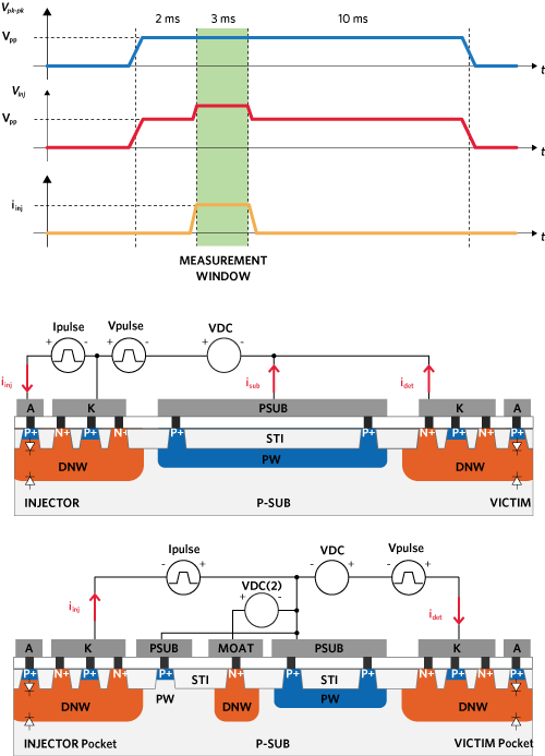
Figure 8. HS injection latch-up test waveform in a wafer-level setup for the pocket-to-pocket voltage VPK-PK, injector voltage VINJ and current IINJ (a). Cross-sections of the latch-up test structure and test setup components for HS hole injectors (b) and LS electron injection (c).
This experimental approach results in measured critical conditions for latch-up dependencies of the critical injection current for latch-up upon the applied injector-victim pocket-to-pocket voltage, as shown in Figure 9. The data correlates with the packaged level results obtained with the industrial tester, the Cadence® Virtuoso® Parameterized Cell Reference, and is comparable with various process options.

Figure 9. Wafer-level and MK2-critical HS and LS latch-up current at 25°C and 125°C upon injector-victim spacings.
Block-Level HV Latch-Up Automated Verification and Co-Design
An essential element of the final co-design approach is automated verification on the block rather than at the top cell level. Based on timeline and resource limitations, verification of a finished IC layout hardly tolerates any major changes. It is important to properly plan and arrange the chip layout blocks at the schematic design level or even at pin specification planning.
To enable the block-level verification, several necessary features must be added in the process design kit (PDK). One feature introduces pad nets used to propagate the information in the netlist about the pad types and voltage levels. It enables both topological and electrical verification components with a tool [7] where the code assigns the extracted devices with the injector or victim roles. For example, an NMOS connected to the pins is checked for a connection to specific pad types, as translated from the pad net. It is assigned to the role of LS injector if the drain is connected to an IO pad type and if the body is connected to a GND pad net type. This diode becomes the injecting junction at a negative current injection realized by pulling down the I/O pin below the ground potential.
This advanced approach enables verification at the stage of incomplete top-cell layout because it does not require full hierarchy and the external pads. With relatively large latch-up rule spacings, a redesign of the verification of a complex HV power IC at the top level can diverge and, thus, become an impractical task. On the other hand, proper planning with iterative real-time verification of incomplete blocks helps to achieve the most space-saving components placement.
The trend toward automatic place-and-route involves a proactive latch-up co-design at earlier steps with pad net cells that combine both layout and schematic properties. The pad type identifies the type of external pad that is connected to the net in the future: IO signal pins, supply pins (VCC), and ground reference (GND) or special functions, such as internally generated supplies. The operating voltage of the pin is defined in the pad net and matches the PDK range for the pocket MOV.

Figure 10. Pad net cell placement schematic example.
When the pad net parameterized cells are recognized as devices in both the schematic and layout views, the verification tool can extract and analyze injector or victim objects. The injector and victim objects can be highlighted in both schematic and layout for co-design decision-making, as shown in Figure 11. The pad net information is propagated throughout the layout view as dictated by the connectivity statements in the verification tool. These statements define how the metal, poly, and silicon are connected. Each net within the layout also has an associated pad net. The voltage from the pad net cell becomes associated with the victims or injectors. Such verification can be run immediately to identify the devices which require placement consideration in the layout in compliance with the latch-up guidelines.

Figure 11. High-side injectors (yellow) and victims (red) flagged in the schematic.
Even though no topological layout input information is present at the schematic level, highlighting these devices in the schematic already enables an appropriate future projection of the layout placement of these devices in layout as a co-design assist procedure. The changes in the schematic itself can be made to reduce the latch-up vulnerability with corresponding interactive result visualization (e.g., an insertion of a series resistor between the injecting device and the external pad). Removing a device from the role of injector eliminates the large spacing requirement.
If the Cadence Virtuoso Layout Suite XL5 is used, a constraint in the schematic to assist with the placements of the devices in the layout can be enabled. For example, two HV-tolerant diodes are identified as an HS injector-victim pair in the schematic (Figure 12). A physical constraint can be added in the schematic between diode 1 and diode 2 and a minimum distance set between them. The constraint is translated to the layout, and the automated placement does not allow diode 1 to be closer than the physical constraint value to diode 2. When the schematic latch-up tool identifies an injector or victim device, for example, a property can be set on that device to place the correct guard ring around the injector as part of the device cell.

Figure 12. Highlighting the instance constraint added to a schematic (left) and distance constraint visualized in the layout of the devices constrained (right).
When the block-level layout is complete and matches the schematic correctly, all the latch-up checks, including the spacing rules, are subsequently evaluated using the instantiated pad nets in the layout database. The schematic owner and the layout engineer can address any errors using the common latch-up terminology developed between the two database views. The identified injectors, victims, and nets can be easily displayed. The location of injectors and victims can be highlighted at the block level in the physical database, as shown in Figure 13.

Figure 13. Block layout showing HS injecting diodes (red) and the final top-level cell.
Figure 14 shows another co-design case example with a simplified HV circuit with two I/O pins and a floating ESDP rail with a core active clamp and floating ESDP rail. Because ESDP is not connected to the power supply, the scenario of HS injection for I/O diodes D1 and D2 is automatically eliminated. The circuit can pass latch-up with the HV injectors (upper diodes) and victims placed at minimum separation space because the RC-time constant of the ESD clamp driver belongs to a shorter time domain than the domain for the latch-up test. However, this space-saving approach can cause a transient latch-up risk if I/O pins have fast transient specification. In this case, the in-rush current through an active clamp results in the diode injection and the spacing rules being followed to avoid latch-up, while the ESDP rail must be updated with the VCC pad net.

Figure 14. Co-design example for floating-supply active clamp injection.
Summary
For HV power analog ICs, latch-up co-design methods have significantly evolved from the traditional LV CMOS I/O and core latch-up basis. The cost-effective HV power IC design requires the advanced approach based on iterative block-level verification with HV latch-up rules that involve new principles to combine both topological and electrical verification of the spacing rules and effective collection rings. Considering the typical 20% to 25% of the area on an HV analog power chip consumed by ESD and latch-up features, the new latch-up co-design methodology is a necessary design paradigm shift to deliver the most optimal IC products in terms of quality and cost effectiveness.
Starting from the pin specification and the block-level schematic sketch, optimal layout planning can be done using a placement strategy that combines the iterative block-level verification for the analysis of the quasi real-time layout options and trade-offs including the circuit redesign options. The approach introduces new opportunities to co-design ICs with pin specifications for system-level, power-on mode ESD and surge at elevated injection current levels and different time domains compared to conventional latch-up. Further evolution of the approach can be focused on rules that would consider the aspect ratio of large distributed injector objects (e.g., power arrays and process technology optimization).
References
- V. A. Vashchenko and A. A. Shibkov. "ESD Design for Analog Circuits." Springer 2010.
- IC Latch-Up Test JESD78E, JEDEC Solid State Technology Association, 2016.
- ISO 10605 Standard, 2008-07-15, ISO, Switzerland.
- ANSI/ESD SP 5.6-2009, “Electrostatic Discharge Sensitivity Testing - Human Metal Model (HMM),” 2009


