A Low Loss Replacement for an ORing Diode
Introduction
ORing diodes are used to connect multiple supplies together to increase reliability (through supply redundancy) or to increase total power. A diode also allows a supply to disconnect if it has insufficient voltage.
At high power levels a Schottky diode is usually chosen as the ORing diode because of its relatively low forward drop (0.35V to 0.6V). But at higher current levels even a Schottky’s forward drop creates significant power loss.
A better alternative is the LT4351 controller, which turns a power N-channel MOSFET into a near ideal diode suitable for high power ORing applications. The low RDS(ON) of the external MOSFET provides for low on resistance when conducting,while the LT4351 maintains a scant 15mV forward voltage across the MOSFET when lightly loaded.
By way of comparison consider a 10A at 5V (50W) supply. Under these conditions, a Schottky diode with a forward voltage of 0.45 (SBG1025L) dissipates 4.5W of power—a 9% efficiency loss. The LT4351 using a power MOSFET with a 3mΩ on-resistance (Si4838DY) dissipates only 0.3W and creates a 0.03V drop. This is only a 0.6% efficiency loss and the voltage tolerance of the supply also improves. The LT4351 works with inputs down to 1.2V, where efficiency improvements are even greater.
My Diode Can’t Do That
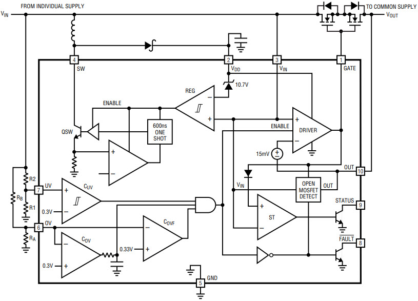
Figure 1 shows the block diagram of the LT4351. In addition to its basic performance advantages over a diode, the LT4351 provides, features that a diode cannot. Input comparators serve to detect an undervoltage or overvoltage input supply and disable the MOSFET switch for an out-of-range supply. The comparators also provide a way to manually turn off power from a supply as well. The FAULT output sinks current during undervoltage or over voltage indicating that the MOSFET is off and an input fault exists.

Figure 1. LT4351 block diagram.
The LT4351 uses an amplifier to drive the MOSFET gate. This amplifier attempts to maintain approximately 15mV across the MOSFET (input to output). If the RDS(ON) of the MOSFET is too large it applies maximum gate voltage and the forward drop is I • RDS(ON). The gate voltage clamps at 7.5V above the lesser of the input or output to help prevent against gate oxide breakdown in the MOSFET. The strong gate drive amplifier can turn off the MOSFET in under 1µs so that minimal reverse current flows in the event of an input short. This strong amp also provides quick recovery from supply glitches.
Either single MOSFETs or back-to-back MOSFETs can be used. Back-to-back MOSFETS are used to block reverse conduction through the MOSFET body diode. A LT4351 with back-to-back MOSFETs disconnects the output from an input overvoltage condition, something a normal diode cannot do.
The UV and OV pins use hysteresis to reduce the probability of triggering a false undervoltage or overvoltage condition. The UV pin uses current hysteresis. When the UV pin drops below the UV threshold ( an undervoltage fault), 10µA of current is drawn from the external resitive divider. This allows the user to set the desired hysteresis level by choosing the appropriate resistor values in the divider. The OV pin has an internal filter that reduces the response to small pulses.
The LT4351 STATUS pin provides indication of the MOSFET state.When the input is greater than the output and the gate to source/drain voltage is greater than 0.7V, STATUS sinks current indicating that the MOSFET should be on. If the input to output voltage exceeds 210mV and the GATE voltage is at its maximum (clamped), FAULT turns on indicating a possible non-functioning MOSFET.
The LT4351 also contains a boost regulator that generates the VDD supply to power the MOSFET gate driver. The boost regulator output current strength allows for quick charging of the VDD supply and supports higher gate drive currents. Thus, the MOSFETs can be turned on quickly during start up and can be quickly turned on and off during normal operation. The regulator only requires a small 4.7µH to 10µH inductor, Schottky diode and capacitor.
Dual 5V Example
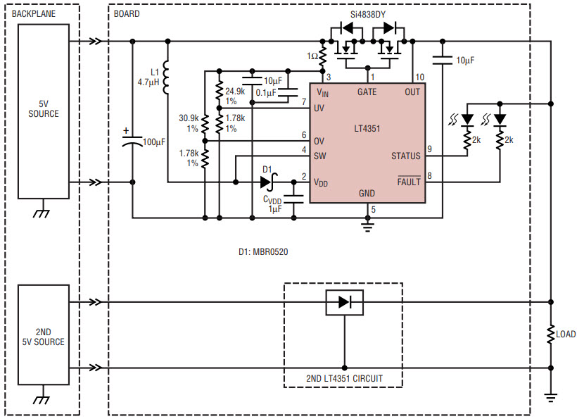
Figure 2 shows an example of a redundant 5V supply. In the event that one supply goes down, the back up supply would take over. In this application, back-to-back MOSFETs are used to prevent the body diode of the MOSFET from conducting in the event that a 5V supply looses regulation and goes into an overvoltage condition.

Figure 2. Dual LT4351 5V ORed supply.
Resistive dividers from IN to UV and OV set the fault detection thresholds. In this example the UV fault occurs at 4.5V with 0.25V of hysteresis and the OV fault occurs at 5.5V.
L1 and D1 are the boost regulator components. The LT4351 creates a VDD supply of 10.5V above IN. If an external supply that can provide sufficient gate drive is available, that supply can be used instead of the boost regulator.
The MOSFETs are sized based on desired voltage drop with considerations for power dissipation. In this case the Si4838DY has a worst case 4.5mΩ RDS(ON) (at temperature) so the back-to-back pair is 9mΩ. These MOSFETs come in SO-8 packages so if power is limited to 1W in each then they can handle 14.9A. The voltage drop across both MOSFETs at this current is 2 • 4.5mΩ • 14.9A = 0.134V. If more current is required, use MOSFETs with lower RDS(ON) and/or better thermal resistance, or add parallel MOSFETs.
The LT4351 is useful in any ORing situation benefiting from low power dissipation—not just redundant supplies. Different types of power sources can also be ORed together, and because the LT4351 diode function is gated, power sequencing of different supplies is relatively easy.
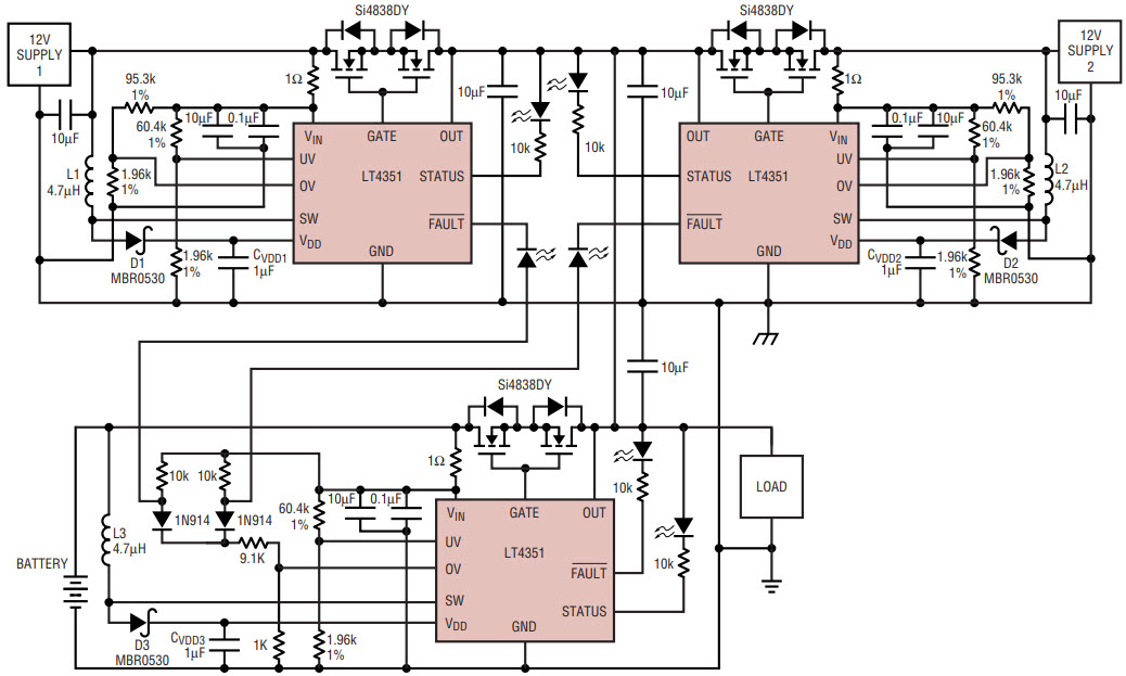
For example, Figure 3 shows a system with two redundant supplies and a battery backup. The two redundant supplies are ORed via the ideal diodes, so power is delivered from the higher of the in-range supplies. Their undervoltage and overvoltage thresholds are set based on the input supply range. The LT4351 circuit for the battery disconnects the battery when power is supplied from either system supply. Its OV pin is above threshold if the FAULT is off on either system supply (UV is set above threshold). If both system supplies are disabled (FAULT of both systems are ow) then the battery’s LT4351 OV pin is pulled below threshold to allow the battery to provide power.

Figure 3. ORed redundant supplies with battery backup.
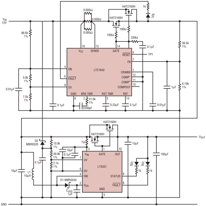
Figure 4 shows an example of combining the LT4351 ideal diode function with a Hot Swap controller. This can be used to create ORed redundant supplies on a plug-in board. The Hot Swap controller provides current limiting, circuit breaker functions and reset timing while the LT4351 provides the ideal diode behavior.

Figure 4. Hot swappable supply with ideal diode.
Conclusion
The trend in today’s power supplies is toward higher currents, lower voltages, higher efficiency and increased reliability. These needs are forcing designers away from traditional Schottky ORing diodes. The LT4351 provides an improved ORing solution by controlling low RDS(ON) MOSFETs to create a near ideal diode. In addition the LT4351 adds increased functionality with supply monitoring that can disable power path conduction. An LT4351 solution has significantly lower power dissipation than a Schottky diode and offers protection features that a Schottky cannot.


